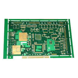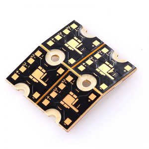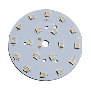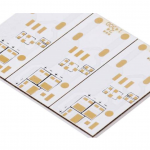


Ceramic circuit boards are actually made of electronic ceramic materials and can be made into various shapes. Among them, the ceramic circuit board has the characteristics of high temperature resistance and high electrical insulation. It has the advantages of low dielectric constant, low dielectric loss, high thermal conductivity, good chemical stability, and similar thermal expansion coefficients of components. Ceramic printed circuit boards are produced using laser rapid activation metallization technology LAM technology. Used in LED field, high power semiconductor module, semiconductor cooler, electronic heater, power control circuit, power hybrid circuit, intelligent power element, high frequency switching power supply, solid state relay, automotive electronics, communications, aerospace and military electronic components.
Unlike traditional FR-4 (glass fiber), ceramic materials have good high frequency and electrical properties, and have high thermal conductivity, chemical stability and thermal stability. Ideal packaging material for generating large scale integrated circuits and power electronics modules.
Key advantages:
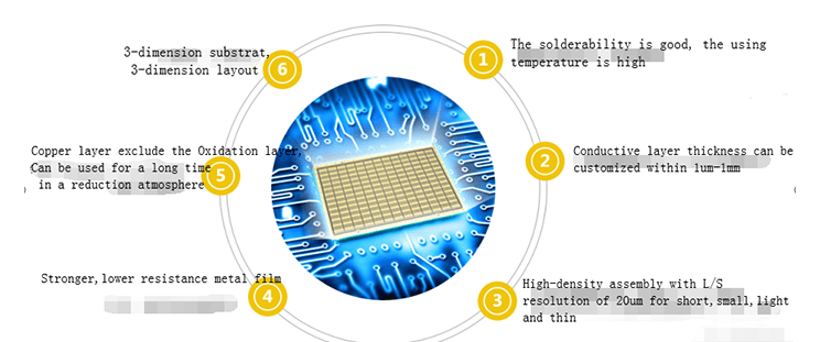
1.Higher thermal conductivity
2.More matched thermal expansion coefficient
3. A harder, lower resistance metal film alumina ceramic circuit board
4. The substrate has good solderability and high temperature.
5, good insulation
6.Low frequency loss
7.Assemble at high density
8. Contains no organic ingredients, resistant to cosmic rays, high aerospace reliability and long service life
9. The copper layer does not contain an oxide layer and can be used for a long time in a reducing atmosphere.
Technical advantages
Introduction to ceramic printed circuit board technology manufacturing process-hole punch
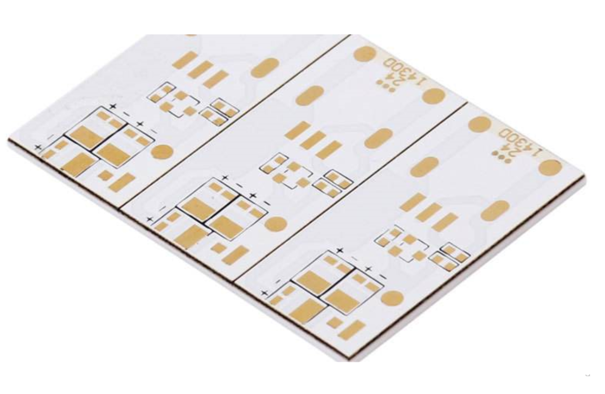
With the development of high-power electronic products toward miniaturization and high-speed, traditional FR-4, aluminum substrate and other substrate materials are no longer suitable for high-power and high-power development. With the advancement of science and technology, the intelligent application of the PCB industry. Traditional LTCC and DBC technologies are gradually replaced by DPC and LAM technologies. The laser technology represented by LAM technology is more in line with the development of high-density interconnection and fineness of printed circuit boards. Laser drilling is a front-end and mainstream drilling technology for the PCB industry. The technology is efficient, fast, accurate, and has high application value. RayMingceramic circuit boards are made using laser rapid activation metallization technology. The bonding strength between the metal layer and the ceramic is high, the electrical properties are good, and the welding can be repeated. The thickness of the metal layer can be adjusted in the range of 1μm-1mm, which can achieve L / S resolution. 20μm, can be directly connected to provide customers with customized solutions.
The ceramic circuit board has a laser drilling process. The bonding force between the ceramic and the metal is high, without falling off, foaming, etc., and the effect of growing together, high surface flatness, roughness ratio of 0.1 micron to 0.3 micron, laser strike hole diameter From 0.15 mm to 0.5 mm, or even 0.06 mm.
Ceramic Circuit Board Manufacturing-Etching
On the copper foil remaining on the outer layer of the circuit board, that is, the circuit pattern is pre-plated with a layer of lead-tin resist, and then the unprotected non-conductive portion of the copper is chemically etched to form a circuit.
According to different process methods, the etching is divided into inner layer etching and outer layer etching. The inner layer etching is acid etching, and the wet or dry film is used as a resist; the outer layer etching is alkaline etching, and tin-lead is used as a resist. Agent.
Basic Principles of Etching Reaction
1.Acidification of acid copper chloride
What is the purpose of ceramics for PCB circuit boards
Acid copper chloride alkalization
Development: The part of the dry film that was not irradiated with ultraviolet rays was dissolved by weakly basic sodium carbonate, and the irradiated part remained.
Etching: According to a certain proportion of the solution, the copper surface exposed by dissolving the dry or wet film is dissolved and etched by the acidic copper chloride etching solution.
Faded film: The protective film on the production line dissolves at a certain temperature and speed.
Acid copper chloride catalyst has the characteristics of easy control of etching speed, high copper etching efficiency, good quality, and easy recovery of etching solution
2. Alkaline etching
What is the purpose of ceramics for PCB circuit boards
Alkaline etching
Faded film: Use meringue to remove the film from the film surface, exposing the unprocessed copper surface.
Etching: Unnecessary underlayers etch away copper with an etchant, leaving thicker wires. Among them, auxiliary equipment will be used. Promoters are used to promote oxidation reactions to prevent precipitation of cuprous ions; insect repellents are used to reduce side erosion; inhibitors are used to suppress the dispersion of ammonia, copper precipitation, and accelerate the oxidation of copper.
New Emulsion: Use ammonia water without copper ion to remove the residue from the liquid on the plate with ammonium chloride solution.
Full hole: This procedure is only applicable to the gold immersion process. Excessive palladium ions in non-plated through holes are mainly removed to prevent gold ions from sinking in the gold sinking process.
Tin stripping: The tin-lead layer is removed using a nitric acid solution.
Four effects of etching
1.Pool effect
During the etching manufacturing process, the liquid will form a water film on the board due to gravity, thereby preventing new liquid from contacting the copper surface.
What is the purpose of ceramics for PCB circuit boards
Pool effect
Ditch effect
The adhesion of the chemical liquid causes the chemical liquid to adhere to the gap between the pipeline and the pipeline, which will cause different etching amounts in dense areas and open areas.
What is the purpose of ceramics for PCB circuit boards
Ditch effect
3. Through effects
The liquid medicine flows down through the hole, resulting in an increase in the rate of liquid medicine renewal around the plate hole during the etching process and an increase in the amount of etching.
What is the purpose of ceramics for PCB circuit boards
Through effect
4, nozzle swing effect
The line parallel to the swing direction of the nozzle, because the new medicinal solution is easy to dissipate the medicinal solution between the lines, the liquid medicine is quickly updated, and the amount of etching is large;
The line perpendicular to the swing direction of the nozzle, because the new chemical liquid is not easy to dissipate the liquid medicine between the lines, the liquid medicine is refreshed at a slower speed, and the amount of etching is small.
What is the purpose of ceramics for PCB circuit boards
Nozzle swing effect
Common problems in etching and improvement methods
Movies are endless
Because the concentration of syrup is very low; the line speed is too fast; problems such as nozzle clogging can cause endless film. Therefore, it is necessary to check the concentration of syrup and adjust the concentration of syrup to a suitable range; adjust the speed and parameters in time; and then clean the nozzle.
2.Surface oxidation
Because the syrup concentration is too high and the temperature is too high, it will cause the surface of the board to oxidize. Therefore, it is necessary to adjust the concentration and temperature of the syrup in time.
3.Thetecopper is not complete
Because the etching speed is too fast; there is a deviation in the composition of the syrup; the copper surface is contaminated; the nozzle is blocked; the temperature is low, and the copper is not finished. Therefore, it is necessary to adjust the etch transfer speed; recheck the composition of the syrup; be careful of copper contamination; clean the nozzle to prevent clogging; adjust the temperature.
4.Etching copper is too high
Because the machine is running too slowly, the temperature is too high, etc., it may cause excessive copper corrosion. Therefore, measures such as adjusting machine speed and temperature should be taken.
|
Article |
Description |
Capability |
|
|
Sercive |
PCB and SMT assembly with one-stop service |
||
|
Material |
Laminate materials |
FR4, high TG FR4, high frequency, alum, FPC |
|
|
Board cutting |
Number of layers |
1-48 |
|
|
Min.thickness for inner layers (Cu thickness are excluded) |
0.003”(0.07mm) |
||
|
Board thickness |
Standard |
(0.1-4mm±10%) |
|
|
Min. |
Single/Double:0.008±0.004” |
||
|
4layer:0.01±0.008” |
|||
|
8layer:0.01±0.008” |
|||
|
Bow and twist |
no more than 7/1000 |
||
|
Copper weight |
Outer Cu weight |
0.5-4 0z |
|
|
Inner Cu weight |
0.5-3 0z |
||
|
Drilling |
Min size |
0.0078”(0.2mm) |
|
|
Drill deviation |
±0.002″(0.05mm) |
||
|
PTH hole tolerance |
±0.002″(0.005mm) |
||
|
NPTH hole tolerance |
±0.002″(0.005mm) |
||
|
Solder mask
|
Color |
Green,white,black,red,blue… |
|
|
Min solder mask clearanace |
0.003″(0.07mm) |
||
|
Thickness |
(0.012*0.017mm) |
||
|
Silkscreen |
Color |
white,black,yellow,blue… |
|
|
Min size |
0.006″(0.15mm) |
||
|
E-test |
Function Test |
100% Functional test |
|
|
PCBA Testing |
X-ray,AOI Test,Functional test |
||
|
Pcb assembly |
one-stop service electronic manufacxturer service |
||
|
Component sourcing |
Yes |
||
|
Certificate |
IATF16949, ISO13485, ISO9001 |
||
|
Delivery time: |
PCB |
3-8days |
|
|
PCBA |
10-20days |
||
|
Tolerance of pcb |
±5% |
||
|
Max size of finish board |
700*460mm |
||
|
MOQ |
NO MOQ (1pcs) |
||
|
Surface Finish |
HASL,ENIG,immersion silver,immersion tin,OSP… |
||
|
PCB outline |
Square,circle,irregular(with jigs) |
||
|
package |
QFN,BGA,SSOP,PLCC,LGA |
||
|
Sub-assembly |
Plastic,metal,screen |
||