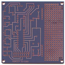
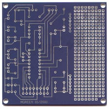
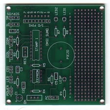
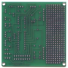
PCB Board Manufacturing is a printed circuit board manufacturing. Rayming is one of the Chinese PCB board manufacturers and has 10 years of PCB board manufacturing experience. PCB features 1-36 layers.

We take internal steps to ensure that the quality of our work meets and exceeds our customers' expectations. The RayMing team utilizes the latest PCB board manufacturing technology and equipment to meet the demand for quality. We are committed to providing quality PCB products and services that help us win the trust and respect of our customers.
We are constantly striving to create innovative solutions, and we spare no effort to purchase the latest PCB board manufacturing technology and experienced labor. This puts us in a good position to provide first-class services from PCB manufacturing to assembly, testing and delivery.
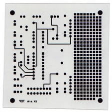
PCB board manufacturing steps
First: PCB film generation
All copper and solder mask films are made from photoexposed polyester films. We generate these movies from your design files to create an accurate (1: 1) movie representation of your design. When submitting Gerber files, each individual Gerber file represents one layer of the PCB.
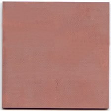
Second: PCB choose Raw material
Industry standard 1.6mm thick FR-4 laminated copper covers both sides. The size of the panel will fit multiple boards
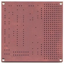
Third: PCB drilling
The through-holes required to create a PCB design come from the file you submitted, using an NC drill and a carbide drill.
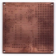
4th time: PCB electroless copper
For the vias to be electrically connected to different layers of the PCB, a thin copper layer is chemically deposited in the vias. This copper will then be thickened by electrolytic copper plating
Fifth: PCB application photoresist and image
In order to transfer the PCB design from electronic CAD data to the physical circuit board, we first applied photoresist to the panel, covering the entire circuit board area. The copper layer film image (step 1) was then placed on the board, and the high-intensity UV light source exposed the uncovered portion of the photoresist. We then chemically develop the circuit board (remove unexposed photoresist from the panel) to form pads and traces.
Sixth: PCB pattern board
This step is an electrochemical process that builds copper thickness in the holes and on the surface of the PCB. Once copper thickness is formed in the circuits and holes, we will plate an extra tin layer on the exposed surface. This tin will protect the copper plating during the etching process (step 7) and then be removed.
Article 7: PCB Strips & PCB Etching
This process takes place in multiple steps. The first is to chemically remove (strip) the photoresist from the panel. The newly exposed copper is then chemically removed (etched) from the panel. The tin applied in step 6 protects the required copper circuits from being etched. At this point, the basic circuit of the PCB is defined. Finally, the protective tin layer is chemically removed (peeled) to expose the copper circuit.
8th: PCB solder mask
Next, we coated the entire panel with a liquid solder mask. Using a thin film and high intensity UV light (similar to step 5), we exposed the solderable area of the PCB. The main function of the solder mask is to protect most copper circuits from oxidation, damage and corrosion, and to keep the circuits isolated during assembly.
Page 9: PCB legend (screen printing)
Next, we printed reference signs, logos, and other information contained in the electronic file onto the panel. This process is very similar to the inkjet printing process, but specifically for PCB design
10th: PCB surface treatment
Finally, a surface finish is applied to the panel. This surface treatment (tin / lead solder or immersion silver, gold plating) is used to protect the copper (solderable surface) from oxidation and to be soldered to the PCB as a component
The 11th: PCB manufacturing
Last but not least, we use NC equipment to route the perimeter of the PCB from a larger panel. The PCB is now complete and will ship to you shortly.

This is a single-sided PCB and double-sided PCB circuit board manufacturing process, and multilayer PCB board manufacturing will be more complicated. Lamination is required.
After 11 PCB manufacturing steps, we will perform 100% electronic test on your PCB board.
We will be a one-stop supplier for all types of PCB, printed circuit board manufacturing and complete turnkey PCB assembly. We specialize in high-level PCBs, engineering PCB prototypes, and a full range of electronic manufacturing services. Each PCB is manufactured to the highest quality standards, including Flex PCB and rigid flexible PCB and circuit board components. Our electronic assembly services are unparalleled in speed, quality and workmanship. From bare circuit boards to box manufacturing and final assembly, we are your primary source, with the most competitive prices in the industry
