There is a key component in the electronics industry called a printed circuit board (PCB). This is a too basic part, making it difficult for many people to explain exactly what a PCB is. This article will explain in detail the composition of PCB and some terms commonly used in the field of PCB.
In the next few pages, we will discuss the composition of the PCB, including some terms, a brief assembly method, and an introduction to the PCB design process.
What ’s a PCB
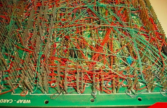
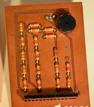
PCB (Printed circuit board) is the most common name, it can also be called "printed wiring boards" or "printed wiring cards". Before the advent of PCBs, circuits were made up of point-to-point wiring. The reliability of this method is very low, because as the circuit ages, the rupture of the line will cause the circuit node to open or short.
Winding technology is a major advance in circuit technology. This method improves the durability and replaceability of the circuit by winding small-diameter wires around the posts at the connection points.
As the electronics industry develops from vacuum tubes and relays to silicon semiconductors and integrated circuits, the size and price of electronic components are also falling. Electronic products are appearing more and more frequently in the consumer sector, prompting manufacturers to look for smaller and more cost-effective solutions. So PCB was born
ComposiTIon (composition)
PCBs look like multilayer cakes or lasagnas-layers of different materials are pressed together in the production by heat and adhesive.
FR4
PCB substrate is generally glass fiber. In most cases, the glass fiber substrate of PCB is generally referred to as "FR4". "FR4" is a solid material that gives PCB hardness and thickness. In addition to FR4, there are also flexible circuit boards produced on flexible high-temperature plastics (polyimide or similar).
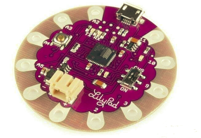
You may find PCBs with different thicknesses; however, most of SparkFun's products are 1.6mm (0.063 ’’). Some products also use other thicknesses. For example, LilyPad, Arudino Pro Micro boards use a thickness of 0.8mm.
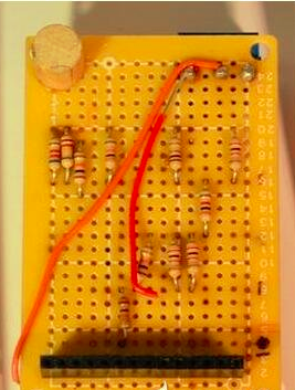
Cheap PCBs and hole boards (see above) are made of materials such as epoxy or phenol, which lack the durability of FR4, but are much cheaper. When welding something on this board, you will smell a big odor. This type of substrate is often used in very low-end consumer products. Phenols have a low thermal decomposition temperature. Excessive welding time will cause them to decompose and carbonize, and emit a bad smell.
Copper
opper. Convert the ounce (oz) per square foot, which is about 35um or 1.4mil copper thickness.
Soldermask (solder mask)
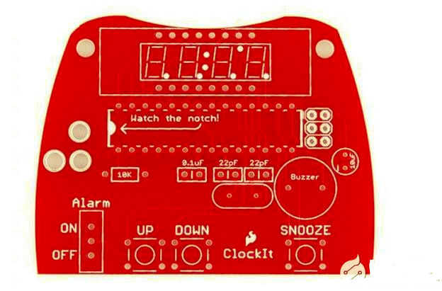
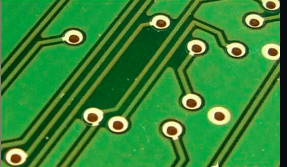
On top of the copper layer is a solder mask. This layer makes the PCB look green (or SparkFun's red). The solder mask layer covers the traces on the copper layer to prevent the traces on the PCB from contacting with other metals, solder or other conductive objects to cause short circuits. The presence of a solder mask layer allows everyone to solder in the right place and prevents solder bridges

In the example in the figure above, we can see that the solder mask covers most of the PCB (including the traces), but the silver ring ring and SMD pads are exposed to facilitate soldering.
Generally speaking, solder mask is green, but almost all colors can be used for solder mask. Most of SparkFun's boards are red, but IOIO boards are white, and LilyPad boards are purple
Silkscreen
Above the solder mask is a white silkscreen layer. Letters, numbers, and symbols are printed on the silk screen layer of the PCB, which can facilitate assembly and guide everyone to better understand the design of the board. We often use the symbols of the silk screen layer to indicate the functions of certain pins or LEDs.
The most common color of the silkscreen layer is white. Similarly, the silkscreen layer can be made into almost any color. Black, gray, red and even yellow silkscreen layers are not uncommon. However, it is rare to see multiple screen layer colors on a single board.
Next page will introduce some common terms in PCB.
Terminology
Now that you know the structure of the PCB, let's take a look at PCB-related terms.
DRC-Design Rule Check.
A procedure to check if the design contains errors, such as short traces, too thin traces, or too small holes.
Drilling Hit-Used to indicate the deviation between the required drilling position and the actual drilling position in the design. Incorrect drilling centers caused by blunt drills are a common problem in PCB manufacturing.
(Gold) finger-An exposed metal pad on the edge of a board, generally used to connect two circuit boards. Such as the edge of the computer's expansion module, memory modules and old game cards.
Stamp hole-In addition to V-Cut, another alternative method of sub-board design.
With a series of continuous holes forming a weak connection point, the board can be easily separated from the imposition. SparkFun's Protosnap board is a good example.
There is a key component in the electronics industry called a printed circuit board (PCB). This is a too basic part, making it difficult for many people to explain exactly what a PCB is. This article will explain in detail the composition of PCB and some terms commonly used in the field of PCB.
Pad-A part of the metal exposed on the surface of the PCB for soldering the device.
There is a key component in the electronics industry called a printed circuit board (PCB). This is a too basic part, making it difficult for many people to explain exactly what a PCB is. This article will explain in detail the composition of PCB and some terms commonly used in the field of PCB.
Puzzle board-a large circuit board composed of many small circuit boards that can be divided.
Automatic circuit board production equipment often has problems when producing small boards. Combining several small boards together can speed up production.
There is a key component in the electronics industry called a printed circuit board (PCB). This is a too basic part, making it difficult for many people to explain exactly what a PCB is. This article will explain in detail the composition of PCB and some terms commonly used in the field of PCB.
Steel mesh-a thin metal template (also plastic), which is placed on the PCB during assembly to allow solder to pass through certain parts.
There is a key component in the electronics industry called a printed circuit board (PCB). This is a too basic part, making it difficult for many people to explain exactly what a PCB is. This article will explain in detail the composition of PCB and some terms commonly used in the field of PCB.
Pick-and-place-A machine or process that places components on a circuit board.
Plane-a continuous piece of copper on a circuit board. It is generally defined by boundaries, not paths. Also called "copper"
There is a key component in the electronics industry called a printed circuit board (PCB). This is a too basic part, making it difficult for many people to explain exactly what a PCB is. This article will explain in detail the composition of PCB and some terms commonly used in the field of PCB.
Metallized Via-A hole in a PCB that contains a ring of holes and a plated hole wall.
The metalized via may be a connection point for a plug-in, a signal change layer, or a mounting hole.
There is a key component in the electronics industry called a printed circuit board (PCB). This is a too basic part, making it difficult for many people to explain exactly what a PCB is. This article will explain in detail the composition of PCB and some terms commonly used in the field of PCB.
Pogo pin-a spring-loaded temporary contact point, generally used for testing or programming procedures.
There is a key component in the electronics industry called a printed circuit board (PCB). This is a too basic part, making it difficult for many people to explain exactly what a PCB is. This article will explain in detail the composition of PCB and some terms commonly used in the field of PCB.
Reflow-melts the solder to connect the pad (SMD) to the device pins.
Silkscreen-Letters, numbers, symbols or graphics on a PCB. Basically there is only one color on each board, and the resolution is relatively low.
There is a key component in the electronics industry called a printed circuit board (PCB). This is a too basic part, making it difficult for many people to explain exactly what a PCB is. This article will explain in detail the composition of PCB and some terms commonly used in the field of PCB.
Slotted-refers to any non-circular hole in the PCB. The slot can be plated or not plated. Since slotting requires additional cutting time, the cost of the board is sometimes increased.
There is a key component in the electronics industry called a printed circuit board (PCB). This is a too basic part, making it difficult for many people to explain exactly what a PCB is. This article will explain in detail the composition of PCB and some terms commonly used in the field of PCB.
In the solder paste layer-Before placing components on the PCB, a certain thickness of solder paste layer will be formed on the pads of surface-mount devices through a steel mesh.
During the reflow process, the solder paste melts, establishing a reliable electrical and mechanical connection between the pad and the device pins.
There is a key component in the electronics industry called a printed circuit board (PCB). This is a too basic part, making it difficult for many people to explain exactly what a PCB is. This article will explain in detail the composition of PCB and some terms commonly used in the field of PCB.
Solder Furnace-A furnace for soldering plug-ins. Generally, there is a small amount of molten solder inside, and the board is quickly passed on it, and the exposed pins can be soldered.
Solder mask-To prevent short circuit, corrosion and other problems, copper is covered with a protective film. The protective film is usually green, or it may be other colors (SparkFun red, Arduino blue, or Apple black). This is commonly referred to as "soldering."
There is a key component in the electronics industry called a printed circuit board (PCB). This is a too basic part, making it difficult for many people to explain exactly what a PCB is. This article will explain in detail the composition of PCB and some terms commonly used in the field of PCB.
Coupling Tin-Two connected pins on the device were mistakenly connected together by a small drop of solder.
Surface Mount-A method of assembly, the device only needs to be placed on the board, and the device pins do not need to pass through the vias on the board.
Hot Pad-refers to a short trace connecting the pad to the plane. If the pad is not properly designed for heat dissipation, it is difficult to heat the pad to a sufficient soldering temperature during soldering. Inappropriate thermal pad design, the pad will feel sticky, and the reflow time is relatively long. (Translator's note, the general thermal pad is done on the side of the plug-in and wave soldering. I don't know why reflow is mentioned in this article. The main consideration of reflow is thermal balance to prevent monuments.)
There is a key component in the electronics industry called a printed circuit board (PCB). This is a too basic part, making it difficult for many people to explain exactly what a PCB is. This article will explain in detail the composition of PCB and some terms commonly used in the field of PCB.
Trace-A generally continuous copper path on a circuit board.
There is a key component in the electronics industry called a printed circuit board (PCB). This is a too basic part, making it difficult for many people to explain exactly what a PCB is. This article will explain in detail the composition of PCB and some terms commonly used in the field of PCB.
V-score-Incomplete cutting of the board can break the board through this straight line. (Translator's Note: Domestically called "V-CUT")
Via-A hole in a board, usually used to switch signals from one layer to another. Plugging refers to covering the vias with solder mask to prevent soldering. Connector or device pin vias are generally not plugged because they require soldering.
There is a key component in the electronics industry called a printed circuit board (PCB). This is a too basic part, making it difficult for many people to explain exactly what a PCB is. This article will explain in detail the composition of PCB and some terms commonly used in the field of PCB.
Wave soldering-A method of soldering plug-in devices. Pass the board at a uniform speed through a melting solder furnace that produces a stable wave. The solder wave will solder the device pins and the exposed pads together.
Next page will briefly introduce how to design your own PCB board.
Designing your own! Design your own!
Do you want to start designing your own PCB. The twists and turns in PCB design are too complicated here. However, if you really want to get started, here are a few points.
Find a CAD tool: In the PCB design market, there are many low-cost or free options. When looking for a tool, consider the following.
Forum support: Do many people use this tool? The more people use it, the easier it is to find an already designed package library for the device you need.
Is easy to use. If it doesn't work, you won't use it.
Performance: Many programs have design restrictions, such as number of layers, number of devices, and board size. Most require you to purchase a license to upgrade performance.
Suppressability: Some free programs do not allow export or migration to other software, limiting you to only vendors. Maybe the low cost and convenience of software is worth the effort, but sometimes it's not worth it.
Go and look at other people's cloth designs. Open source hardware makes this easier.
Practice, practice, or practice.
Keep expectations low. The first board you design may have many problems, but the 20th one may be much less, but there will still be some problems. But you have a hard time clearing everything.
The schematic is very important. Trying to design a PCB board without good schematic support is futile.
Finally, talk about the benefits of designing your own circuit board. If you plan to participate in one or more established projects, the benefits of designing a circuit board are obvious. Compared to designing circuit boards, point-to-point wiring on breadboards is too difficult and the reliability is relatively low. And if your design is good, you can buy your design for a good price 🙂
