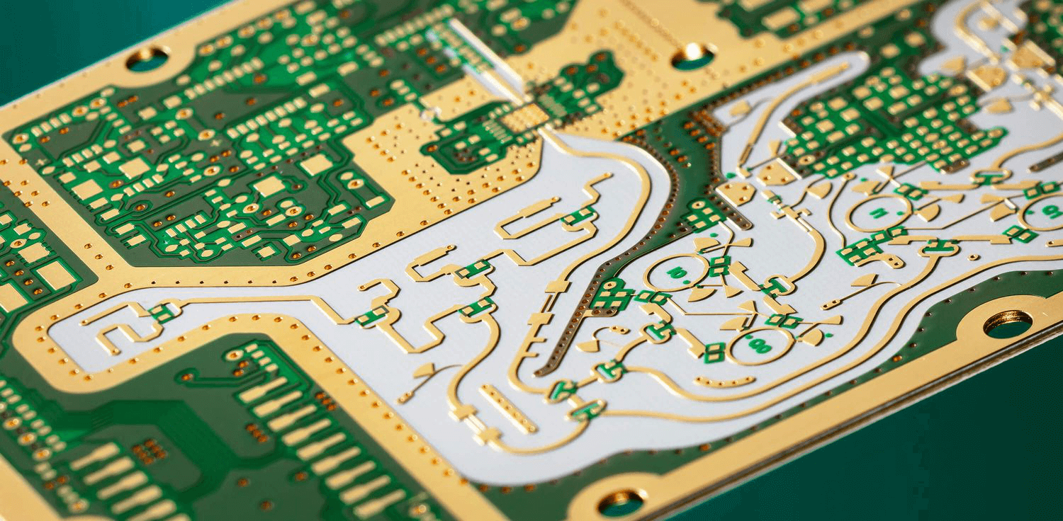
Design Considerations of the Ultra Thick Copper PCB
Ultra Thick Copper PCB incorporates copper foil thickness of 8.6oZ, 11.4oZ, 14.3oZ, and 20oZ among others. The amount of copper in these boards greatly depends on the consumer requirement. Thus, these boards have the ability to generate effective results.
They are robust and efficient. They can enhance the overall life of the electronics. Consumers use them in places that require high-maintenance. The boards have the ability to withstand extreme weather. There is no denying their importance. Thus, we have come up with a complete guide on ultra-thick copper boards.
General Design Considerations
For starter, let us focus on the basic design concept. Several factors need consideration during the design phase. These factors will have a major impact on the performance and reliability of the electronics.
Below, we did list the minimum number of factors required for a reliable PCB. You can find the list of all factors in the IPC-2221. Also, the guidelines provide information about their performances and tradeoff.
Electronic Requirements
The manufacturer should collect all end-product requirements before the design phase. After all, these requirements will influence the design greatly. As a manufacturer, you need to focus on the environment the product
In addition, you need to see its servicing and maintenance. These factors will affect the board size, part placement, and coating. It will also influence the marking, conductor routing and the final finish.
Performance Consideration
You should ensure that your boards meet or exceed the requirements established by IPC-6011. In general, the IPC-6011 has established three basic performance classes for an end-product.
Class One focuses on the general electronics product. The second class, on the other end, is about the dedicated service electronics product. The last class ‘Class 3’ is all about products that require a high-reliability rate.
Properties and Material Type
You will have a wide range of product materials at your disposal. You can choose from standard PCB epoxy resins to a material with more specialized properties. However, the type of properties you choose depends on the end-product.
Some of the common properties include electrical properties and the flame resistance. The temperature, structural strength and the machineability are included. In addition, thermal stability, thermal conductivity, and CTE are important properties.
To choose the right laminated material, see the ones listed in IPC-4101. An important thing to focus on is the temperature rise of high current designs. Therefore, ensure that the temperature does not exceed the maximum operating temperature of the laminate material.
If the temperature exceeds then the operation temperature, it will lead to failure. You can discover the operating temperatures of different laminate materials in IPC-2222. You should specify the material you use. Also, mention the minimum dielectric thickness on the master drawing.
Ultra Thick Copper PCB: Electrical Insulation
For electrical insulation properties, you will use the solder-masking technique. Ensure that the technique generates effective results. A good idea is to folly the solder mask coating guidelines by IPC-SM-840. With the right solder masking, you can protect vias from soldering and process solutions.
This would enhance the overall life of the Ultra-Thick Copper PCB. For effective tenting, the maximum finished hole should be 0.025”. For larger holes, you should talk to the consumer. If they agree, you can increase the size of the hole.
In the case of solder mask’s electrical insulation properties, you should focus on the type of mask and its thickness. For greater electrical insulation, properties use the capping process or similar processes. The end-user should specify al the legends and marking on the master drawing.
They should clearly specify the type of marking. For instance, etched characters, non-conductive ink among others. Ensure that marking is never on the conductive surfaces. It should not be covered by the components.
The consumer should place marking with the revisions, layer numbers, part number etc. For non-conductive inks, they can be liquid screened. Mark them within 0.020” to 0.005” or more from the solderable surface. However, do remember that liquid screened markings lead to high surface irregularities.
Destructive Quality Evaluations
To indicate the destructive quality evaluations, use coupons. These evaluations do not exist on the PCB. Below are the process parameters that need evaluation.
- Each Layer’s Copper thickness
- Layer to layer registration
- Plating adhesion
- In pated through holes
- Soldermask thickness
- Solderability
- Solder mask adhesion
Manufacturers usually use the sampling technique to ensure material quality. In general, the material manufacturer is responsible for assuring the quality of its product. The master drawing should mention all the material.
Thus, the manufacturer should ensure that all the materials are according to the ones specified in the drawing. The end-user needs to outline the conformance evaluation procedure. In addition, the drawing needs to have the configuration to allow the coupon to undergo conformance evaluation.
Final Finishes
Below are some important final finishes.
Hard Gold: - Used for the Edging of the board contacts. It is the cobalt hardener or the nickel hardener over the electroplated nickel.
Hot Air Solder Leveling: - To cover the bare copper, dip it in a bath of molten solder. To remove the excess solder, use the hot air knives.
OSP: - OSP offers protection to the underlying plating. It does not let it oxidase. In addition, it is effective to flatten the surface mounts. If you use OSP, make sure that you discuss it with the client. Agree on the storage life and solderability retention.
ENIG: - The electroless nickel is covered with immersion pure gold. The manufacturer chemically applies it. The manufacturers use it to prevent oxidation. In addition, they apply it for wire bonding.
Immersion Tin or Sliver: - It is the perfect solution for an affordable ROHS compliant finish.
Inspection and Traceability
High-quality Ultra Thick Copper PCB manufacturer compete to in-process inspections. In addition, the final inspection would be according to the one listed on the master drawing. Below are the things that are part of the finished product’s evaluation process.
- Process control evaluations
- Conformance inspections
- Material
Electrical Testing
The manufacturer uses a number of electrical testing for bare boards. For instance, dielectric withstanding voltage, insulation resistance, and continuity testing. Other includes conductor resistance, and capacitance is common to test available.
As a manufacturer, ensure that all your testing is in accord with IPC-9251. There are certain tests that are difficult to perform. However, sometimes you will have to conduct these tests. Conduct them only if the client requests them.
Board Size and Type
Several factors contribute to the board size and type. For example, a number of layers, circuit complexity, and copper weight. You also need to pay heed to pallet size and the process parameters. However, do remember to consult your client on the board size.
Documentation
Ensure that the documentation contains a copy of the master drawing. You can keep the data in either hard copy or soft copy. To identify the electronic files or the documents, use the revision status and the board part number. Also, add important notes to the revision for better understanding.
Take Away
Following the design guidelines for Ultra Thick Copper PCB will help you develop reliable PCBs. Having a proper design would help you identify issues before the hand. Therefore, Hua Feng Circuit spends quality time in the designing phase.
After all, they would have all the virtual knowledge about the PCB via the master drawing. In addition, it helps eliminate potential designing and developing errors. It provides transparency between the employee and the employer.
