All About Thick Copper PCB Manufacturer
Thick Copper PCB Manufacturer - The thick-copper technology allows complex switches to mount in limited space with higher current levels.
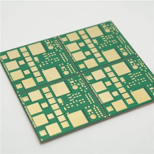
This PCB, made in authentic etching innovation is the main decision when high flows are unavoidable. Structures describe thick copper PCBs with copper thicknesses from 105-400 µm. These PCBs are utilized for enormous (high) current yields and for streamlining of the thermal administration. The thick copper permits enormous PCB-cross-segments for high currents and empowers heat scattering. The most well-known structures are multilayer or twofold sided. With this PCB innovation, it is additionally conceivable to consolidate fine format structures on the external layers and thick copper layers in the inward layers.
Thick Copper PCB Manufacturer items are utilized widely in power electronic gadgets and force supply frameworks. A developing pattern in the PCB business, this interesting sort of heavy copper PCB highlights a completed copper weight of more than 4oz, contrasted with the 1- 2oz (0μm) copper weight commonly found in those with a standard PCB copper thickness.
The extra copper PCB thickness empowers the board to direct a higher current, accomplish significant heat appropriation and actualize complex switches in a restricted space. Different favourable circumstances incorporate expanded mechanical quality at connector locales, the capacity to make a small item size by fusing various loads on a similar layer of hardware and the ability to utilize extraordinary materials to their most extreme limit with an insignificant danger of circuit failure.
Thick Copper PCB Manufacturing
The highlights of thick copper PCBs have principally required in the power electronic gadgets and centralpower framework.
- Thick Copper PCB Design Concerns
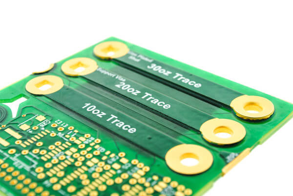
The width and copper loads are the critical parameters for electrical specialists while structuring a thick copper PCB. These two highlights decide the current-conveying limit of the thick copper PCB. For PCB makers, high-current is a test because their reasonable burden connects to security concerns. Besides, the bind cover process requires strict control during the procedure because the measure of copper thickness is more noteworthy than the substrate thickness.
Plus, the assembling procedure, for example, design etching, boring, and overlay process, additionally should be deliberately controlled during the assembling of thick copper completed PCBs. The thick copper PCBs are made with various copper loads on little impressions.
In PCB copper-producing, the design has an essential job since it helps in decreasing danger and evades the excessive cost, which results from complex PCB structures. Thick Copper completed PCB's offer enduring wiring answers to satisfying the prerequisites of better thermal administration frameworks.
They direct the ideal power and extra thermal dissemination. Suitable least weight, measurement, kinds of the segments and materials, and separating are the three plan parameters that must be checked.
Thick Copper PSB Fabrication
Smooth and continuous correspondence between electronic plan and assembling engineers bring effective PCB manufacture. Configuration engineers must know about the maker's detail, for example, limit, dispersing, through width, and square foot size, and so forth. Furthermore, PCB type prerequisites must be mulled over like force, through the opening structure, and material.
For thick copper PCBs, the manufacturing technique is like standard FR4 PCB. Creating thick copper printed circuit boards includes drawing and plating forms like rapid plating and deviation scratching. The fundamental objective is to remember a copper thickness for sidewalls and openings.
During the creation procedure, when the printed circuit board is dependent upon a few cycles, the plated gaps may get frail. In a perfect world, the openings reinforce when thick copper include. That is the reason in electrical circuits; it is desirable over pick outrageous flow and force applications.
It is conceivable to join Thick Copper PCB Manufacturer to the conventional board consistently. Without further ado, previously, producers attempted to build thick copper PCBs with the carving procedure as it were. Creation of scarcely any circuit boards experienced from scrap right now of over-scratching edge and lopsided edge lines.
To keep away from this, later, propelled drawing and plating procedures were applied to accomplish the ideal carving edge and straight edge. During Thick Copper PCB creation, the amassing of cooling balances is of high noteworthiness.
Thick Copper PCB edges
Easy Implementation: Even inside the little spaces, they are anything but difficult to execute in the mind-boggling switches. Thick Copper PCBs evacuated the requirement for mind-boggling and massive metal bars or wires.
Thermal Distribution: The specialists can work with the outrageous warm obstruction due to the copper-plating of these PCBs whenever. Perfect thermal administration and unwavering elite quality are the real purposes behind their popularity.
In harmful situations like temperature vacillations, Thick Copper completed PCB is to depend upon. For instance, the mechanical obstruction of PTH and agreement focuses increments too in surrounding temperatures.
Thermal Dissipation: Overheating can flop any electrical framework whenever. Here, thick copper circuit boards assume their job. They help in keeping away from conceivable overheating. This component assists with keeping up the temperature of the entire framework effectively to the ideal levels. The circuit board scatters the Thermal successfully, consequently, guarantees ideal circuits execution.
Fascinating Material: Sometimes, the electronic segment planning requires the utility of wrong materials. In this manner, we are utilizing a thick copper circuit board to secure and improve such materials.
High Current Conduction: In the electrical business, thick copper printed circuit board help in excellent flow conduction. The printed circuit boards interface various sheets together to ensure inordinate current can't cut indiscreetly. Thick Copper completed PCB's have the best present conveying limit and capacity.
Mechanical Strength: The full mechanical quality of the thick copper loads circuit board is in a perfect world great. This component makes a robust and strong electrical framework all in all.
Heat Sinks: Thick board PCB give the locally available heat sink, which is a fundamental part of electrical and electronic frameworks. On mosaic surfaces, it is anything but difficult to accomplish reliable and successful warmth sinks. The heat moving technique between layers decreases the expense.
Thick Copper PCB Applications
Understanding the application necessity is fundamental before selecting the thick printed circuit boards. It's anything but another development. They have been utilized in creating resistance and military utilization of weapon control frameworks. Thick Copper PCBs are ordinarily utilized in underneath referenced regions:
- Military applications like siphoning plants stockpiling.
- Rail footing and sign and safety framework applications in the car business.
- With thick mosaic layer, they utilize as planar transformers.
- In beat converters, they are extremely popular as they help in creating littler transformers with the inductance of low winding break.
- They utilize as sun-based force converters in sun oriented board.
- Intensification framework and torque control applications.
- Assurance and overhead transfers in electrical force frameworks.
- Cooling High force frameworks.
- UPS frameworks in the media transmission industry.
With the expansion in PCB innovation and multifaceted nature, electronic specialists need to focus on PCB configuration rules and assembling strategies. Along these lines, the item can accomplish the ideal harmony between cost, execution, prerequisite, and security. The advantages of features lead to the least assembling dangers.
Benefits of Thick Copper PCB
- High flows and thermal dispersal in the circuit board.
- Directed incomplete increment in cross-area for high-current ways.
- Decrease of room prerequisites for high-current conductor frameworks.
- From test to arrangement creation from a single source.
- Force and control gadgets on a solitary board.
- PCB creation and handling with standard materials and arrangement forms.
- Cost improvement of the final item.
