A Comprehensive Introduction to Heavy Copper PCB
The every evolving PCB industry has led to the designing and development of heavy copper PCB. These Printed Circuit Boards offer endless benefits. Due to these benefits, a large number of electronics use them.
They ensure high performance and long shelf life. Even though these PCBs are expensive, yet they are popular due to their effectiveness. In the course of the article, we will provide you with a brief introduction of the Heavy Copper Printed Circuit Boards.
Introduction
There is no formal definition available for Copper Printed Circuit Boards. They are like the regularly printed circuit boards. However, they feature 3 ounces of copper in both the external as well as internal layers.
The addition of copper is what makes them stand out. So, in simple words, Heavy Copper Printed Circuit Boards are any PCBs that have a copper thickness of more than 4 Oz/ft2. There is another form of Copper PCB, Extreme Heavy Copper Printed Circuit Board. The amount of copper present in these boards is way more than the Heavy Circuit Boards.
Copper PCBs are reliable. As use the through-hole circuit technique, a thicker plating, and an appropriate substrate. The reliable wiring platform uses robustness. Also, manufacturers use a wide variety of plating and etching techniques. Using these techniques they able to produce a variety of PCBs.
The main goal is to add copper thickness via plated sidewalls and holes. If the PCB manufacturer successfully does that, it can create a reliable PCB.
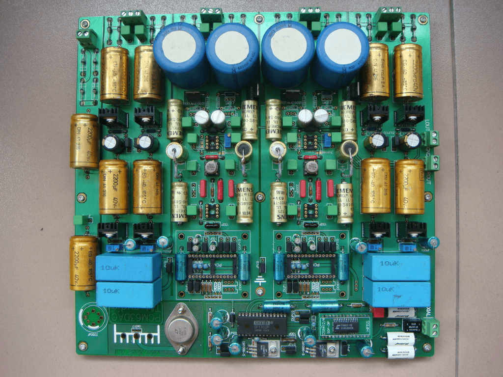
Heavy Copper Circuit Construction
The manufacturer uses several different plating as well as copper etching processes to design Printed Circuit Boards. Even if they are design or developing double or single-sided PCBs, they still use these techniques.
The circuit comprises of several layers. You will find copper foil(thin sheets) as the starting of the circuit layers. Generally, the weight of the copper foil is between 0.5Oz/ft2 to 2Oz/ft2. To remove the unwanted copper, you would have to etch these sheets.
Next, comes the platting. With plating, you add the desired amount of copper thickness. You can define a copper thickness in several parts including pads, traces, etc. To ensure the lamination of all circuit layers, use a reliable substrate. For the substrate as an epoxy base, you will mostly use polyimide or FR4.
The same technique holds for heavy copper boards. However, instead of using standard etching and plating processes, you need specialized processes. Manufacturers tend to use specialized plating as well as itching techniques.
These techniques are advance in comparison to the standard ones. Thus, they can generate better are more refined results. Differential etching and high speed or high step plating are common examples of specialized techniques.
Initially, the formation of Heavy Copper PCB involved the etching laminated board material i.e., thick copper. People did manage to develop PCBs, but they were not reliable. They had unacceptable undercutting and sideways had uneven traces.
Fortunately, today we have advance plating technology. Due to this advancement, you can now develop copper PCB using a different etching as well as plating methods. Thus, the result is excellent. Consumers can generate negligible undercuts and straight sidewalls.
Copper Circuit Board Plating
To increase the copper thickness on the board, you would need the plating process. The process allows the fabricator of the board to acquire the desired copper thickness. You can define the plated holes’ copper thickness, sidewalls, and vias.
The great news is that you can use the standard features with heavy copper on a single board. The manufactures call this board, the PowerLink. There are several advantages to this board. Some of the benefits include a smaller footprint and fewer layers.
Also, it has a less impedance power distribution. It is also extremely cost-efficient. Generally, you would have to use a separate board for control circuits with high power and their control circuit. However, this is not the case with the copper board.
You can integrate control circuits and high-current circuits on the same board. The heavy copper plating offers high density, yet a simple and reliable board structure. It helps you come up with robust and reliable Printed Circuit Boards.
You can seamlessly connect features of a heavy copper board to a standard board. This way, you will get the best of both worlds. The simplicity of a standard board and efficiency of a copper board. Nonetheless, you to discuss the design and the fabricator process with the manufacturer.
This will help you understand the design and development capacity of the manufacturer.
Benefits of Heavy Copper Printed Boards
Below, we have come up with the benefits of heavy copper printed boards.
- Copper boards then to offer high thermal endurance capacity in comparison to standard boards.
- Their excellent carrying capacity further enhances their appeal.
- They come with high mechanical strength in the PTH holes.
- Since they combine several copper weights in the same Printed circuit Boards, thus they tend to reduce the circuit size.
- It has high and enhanced mechanical characteristics due to the usage of exotic materials.
- It offers high thermal resistance due to the copper-plated vias.
- They offer high mechanical strength in connector sites.
- You will not have to bear with convoluted wire bus configurations.
- The places that have heavy copper act as heat sinks. They can be an interface to cold plates.
Heavy Copper PCB Application
Due to its unlimited features, you can heavy copper Printed boards everywhere. Nonetheless, below are the most common applications that incorporate copper PCB.
- HVAC Systems
- Overload Relays
- Protection Relays
- Rail Traction Systems
- Power Line Monitors
- Safety and Signal systems
- Torque Controls
- Solar Power Converter
- Circuit Board Strength and Survivability
Thermal Management
When it comes to the circuit board’s substrate, the manufacturer has many options. They can choose standard FR4 or they can go with polyimide. The FR4 operating temperature is 130 degrees C. On the other hand, polyimide’s operating temperature is 250 degrees C.
To determine the thermal integrity of a finished PCB, the manufacturer uses different methods. However, do remember that the assembly process, various board fabrications, and repair processes act as thermal strains. A good way to check thermal integrity is to use thermal cycle testing.
The TCT helps you understand the ability of the board. It makes the board undergo air to air thermal cycling from 25 degrees C to 260 degrees C. This will help check the increase in the resistance of a circuit. The increase in resistance is often responsible for the breakdown. Thus, the manufacturer needs to contain it.
With the TCT, manufacturers can determine the failure rate. Also, the test shows that the failure rate is unacceptable. Regardless, the material you use for a PCB, it cannot fail. Therefore, you should use heavy copper circuits. They would ensure the removal of such failures.
If you incorporate 2Oz/ft2, it would reduce the failure rate to almost zero. So, it is a good idea to use heavy copper circuit boards.
Takeaway
Heavy Copper PCB is famous because it offers excellent thermal management and reliable performance. These circuit boards can meet the demand of modern electronics. That is, they can effortlessly pass-heavy current without causing any short-circuiting.
In case, you are still wondering about the benefits of heavy copper circuits, reach out to our experts. We, CCTC-HFPCB, ensure the optimum performance of the circuits. Our experts will help you make the right decision in terms of choosing circuit boards for your electronics.
