Major development trends in thick printed circuit board technology
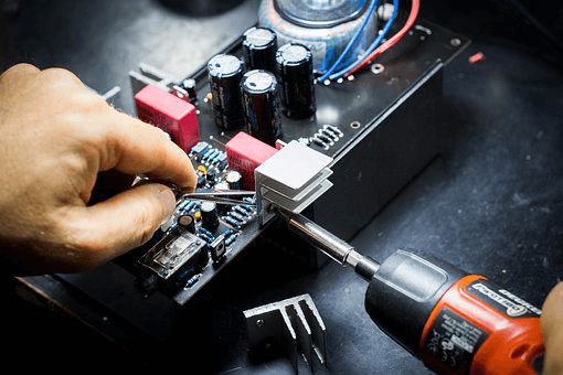
Table of Contents:
- Heavy Copper PCB Manufacturer contribution to Technology Industry
- Is there a difference between gold plating and immersion gold on heavy copper PCB?
- What is the difference between gold plating and immersion gold on heavy copper PCB?
- How Does a Heavy Copper PCB Manufacturer measure the thickness of a PCB?
- Thickness Variations in Heavy copper PCB manufacturing
- Relationship between heavy copper PCB foil thickness, line width, and maximum load current
- Heavy copper PCB specifications on a per square foot (ft 2 )
Heavy Copper PCB Manufacturer contribution to Technology Industry
In the 21st century, Heavy Copper PCB Manufacturer has entered a highly information-oriented society, and PCB is an indispensable and important pillar in the information industry.
Electronic devices require high performance, high speed, thinness, and brevity. As a multidisciplinary industry, PCB is the most critical technology for high-quality electronic devices. PCB products have made a major contribution to high-quality electronic devices, regardless of rigid and flexible combined multilayer boards and module carriers for IC package substrates. Furthermore, the circuit board industry occupies an important position in electronic connection technology.
Is there a difference between gold plating and immersion gold on heavy copper PCB?
Heavy Copper PCB Manufacturer plays a very important role in PCBA-SMT processing. There are many process requirements for circuit boards. For example, customers often request gold plating and gold immersion. Therefore, these two methods are commonly used for PBC cards. Similarly, it seems the names are similar, but in fact, there is a big difference. Many customers usually cannot tell the difference between the two processes.
What is the difference between gold plating and immersion gold on heavy copper PCB?
Introduction of gilding and immersion gold:
Gold plating: Gold particles are mainly applied galvanically to printed circuit boards. Due to the strong adhesion of the gilding, it is also called hard gold. Subsequently, the golden fingers of memory sticks are hard gold, high hardness and wear resistance.
Sinking gold: A plating layer is created by a chemical oxidation-reduction reaction process, and gold particles crystallize and adhere to the PCB pad. Because of its poor adhesion, it is also famous for soft gold.
The difference between gold and immersion gold:
- Heavy Copper PCB Manufacturer carries the gilding process before the solder mask in the chip processing. It may appear that green oil has not been cleaned and is not easily tinned. The gold immersion process takes place after the solder mask and the chip is easy to the tin.
- Before a PCB manufacturer carries the gilding process, it requires a layer of nickel usually. Similarly, it follows a layer of gold. The metal layer is copper-nickel-gold because nickel is magnetic and affects the shielding of the electromagnets. The immersion gold process dips gold directly into the copper skin. The metal layer is copper-gold, with no nickel and no magnetic shielding.
- The gold plating differs from the immersion gold and the crystal structure formed is not the same. Immersion gold is easier to weld than the gold plating and does not cause welding errors. In addition, immersion gold has a denser crystal structure than gold plating and is less susceptible to oxidation.
- The flatness of the gold-plated circuit board is not as good as that of sinking gold. According to Heavy Copper PCB Manufacturer, flatness is better for panels with higher requirements. Falling gold is generally used, and falling gold generally does not occur after assembly.
How Does a Copper PCB Manufacturer measure the thickness of a PCB?
Generally, a Heavy Copper PCB Manufacturer measures the thickness of a PCB in terms of weight (ounces). For example, a 1-ounce copper layer means that it is 35um thick, or 1.4mils. Measurements refer to 1 ounce (28.35g) of copper being evenly covered over 1 square foot (929 square centimeters) of the PCB area.
Therefore, "heavy copper" refers to a thicker copper conductor layer. Generally, the copper layer of the PCB starts as a solid "sheet" of copper (copper foil, some layers of the foil are purchased by the manufacturer as raw materials. And other layers can be pre-laminated on glass fiberboards), and the overall thickness is uniform.
Most of these start out thin-18um to 35um. Once Heavy Copper PCB Manufacturer drills the PCB, the copper plating process begins to plate the inside of the drilled holes. Sometimes thick PCB manufacturing companies perform drilling before etching and sometimes after. It really depends on the number of layers and the lamination order. Sometimes plating comes before etching, but if the plating process comes before etching, most of the copper will vanish away.
Thickness Variations in Heavy copper PCB manufacturing
A Heavy Copper PCB Manufacturer can carry platting by following methods:
- traces of the PCB-by applying a mask to resist the plating material, whether it is copper, nickel, gold or other metals.
- Heavy copper PCBs may have several layers of thick copper plating.
- Some thicker layers look like a small "wall" on the PCB. 20 oz-30 oz is not a rare thickness. It is significantly thicker and greatly increases the current carrying capacity and thermal mass of the PCB.
Some boards have a 100% solid metalcore. This can also be copper. Compared to thick electroplated plates, copper core plates are very heavy and remove heat very well. These are called "MCPCB" or metal core PCBs and are different from "heavy copper" PCBs.
Relationship between heavy copper PCB foil thickness, line width, and maximum load current
The current-carrying capacity of a PCB depends in principle on the cross-sectional area and temperature rise of the copper berth section of the trace. But the cross-sectional area directly depends on the width and thickness of the line.
Assuming a 10-mil line width 1oz trace can withstand 1Amp under the same 10 ° C temperature rise condition, Heavy Copper PCB Manufacturer should be sure that a 50mils line width trace can withstand greater current than 1Amp.
“But Will it be 5Amps in multiples?”
The answer seems to be no. First, refer to the MIL-STD-275 form. The maximum current it can withstand is only 2.6Amps.
Heavy copper PCB specifications on a per square foot (ft 2 )
with a few ounces (oz) to define, so we often say 1oz (ounces) per square feet is (ft 2 has 1oz on) Weight. The thicker the copper skin, the heavier it is. Because the weight of the copper skin is proportional to the thickness, the ounce of the copper skin can be equivalent to the thickness and can be converted into millimeters (mm) or milli-inches (mils). This is actually similar to how we use pounds when calculating paper. If you are interested, check it out!

Here are a few commonly used sizes that are converted into mils and millimeters for your reference:
0.5 ounces (oz) = 0.0007 inches (inches) = 0.7 mils = 0.018 millimeters (mm)
1.0 ounce (oz) = 0.0014 inch (1.4) = 1.4 mils = 0.035 millimeter (mm)
2.0 ounces (oz) = 0.0034 inches (inch) = 2.8 mils = 0.070 millimeters (mm)
Although Heavy Copper PCB Manufacturer suggests that there are formulas that can directly calculate the maximum current load capacity of copper foil, it will not be so simple when actually designing the circuit. Because Trace's current load capacity is not only related to the cross-sectional area and temperature of the copper foil, other factors such as the number of components on the line, the pads, and vias have a direct relationship.
