Diana Zuckerman and other senior staff. I would cry before I had to take a shower or walk to the car, nevermind if I had to https://africarx.co.za/buy-kamagra-effervescent-south-africa.html really do something!
An Ultimate Guide for Multilayer Pcba Manufacturer to build a perfect Printed circuit board assembly
Table of contents:
1.The idea behind Hdi Pcba Manufacturer
2.History of HDI PCB
3.Industries using HDI boards
4.Comparison with typical circuit boards
5.Features of High dense Hdi Pcba Manufacturer boards
6.Types of HDI boards- Hdi Pcba Manufacturer
7.Hdi Pcba Manufacturer Laser technology
8.Hdi Pcba Manufacturer driving forces
9.Why Hdi Pcba Manufacturer test or verify the board?
10.How do Hdi Pcba Manufacturer plan before fabrication?
11.Conclusion
The idea behind Hdi Pcba Manufacturer
HDI stands for high density interconnect. Technology now covers all over the world. It is important to replace old things with new and reliable. Thus, high density interconnects (HDI) is a type of PCB, with advance material. Generally, a Hdi Pcba Manufacturer develops it.
History of HDI PCBa
The idea of High-Density Interconnect technology came at the end of the 20th century, which means that this technology had been introduced a long time ago.
This technology was first established in the U.S, then adopted fully all over Asia mainly by Multilayer Pcba Manufacturer in china.
This was a bit confusing that the idea of this technology spread in Asia quicker than in the U.S. Subsequently, the U.S was not working more on Multilayer Pcba Manufacturer.
Taiwan Hdi Pcba Manufacturer although was using HDI boards in cellphones, video recording cameras and in computer devices and making more consumers because of HDI products.
Similarly, Happy Holden, Odense, Denmark is the father of HDI. They have worked on a lot. They tell about the management of these boards.
Trending Hdi Pcba Manufacturer
The reader survey tells that the High-Density Interconnect board is the main technology and half of the business is the production of HDI boards. Moreover, High-Density Interconnect Multilayer Pcba manufacturers are more in demand.
Industries using HDI boards
Many industries use High-Density Interconnect board as
- IT and Telecommunicating industries
- Automotive industry
- Consumer Electronics industry
- Industrial electronics
- Global analysis industry
It is a common fact that using High-Density Interconnect boards in these industries approximately 25 % of their business grows.
Hdi Pcba Manufacturer Market trends
All the communication devices, computer devices, electronic devices use High-Density Interconnect boards in markets. Because one HDI board can cover the functions of several PCBs used in a single device.
Similarly, as designers and Hdi Pcba Manufacturer recommend an all in one thing, mean a single small thing having all the functionalities.
Comparison with typical circuit boards
The old printed circuit board and HDI boards are not the same anymore.
| PCB (typical circuit board) | HDI (high density interconnect boards) |
| It has power failure issues | It gives Higher wiring density |
| may face soldering issue | has Fine spaces and lines on the board |
| The holes are done manually by drill heads | The Holes are done by laser drill technology using UV layer and resin copper |
| The VIAs are naked (can be seen on the board) | has Minor VIAs which are Blind/buried VIAs |
| It may be chemical leakage due to contamination | It has Higher connection pads |
| shows the poor quality of signals | provides Faster signals |
| It may cause bending and breakage issues | It has More components on both sides |
| constitutes of 8 layers (a thick stack) | has Smaller geometry with 4 layers and Decreased size, miniature quality |
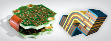
Features of High dense Hdi Pcba Manufacturer boards
Following are the features or High-Density Interconnect boards
- It has a high dense circuit board and higher wiring density
- It connects the layers by metallization
- Advance PCB technology with Hdi Pcba Manufacturer
- It has advanced packaging
- The spaces and line used in the board are less than 100 µm
- micro VIAs are less than 150 µm
- The capture pads used are less than 400 µm
- Layers are in the form of pairs
- More flexibility in the design
- It has a stable voltage rail
- has the least stubs used
- It shows lower EMI
- has a distributed capacitance all over the board
Benefits of Hdi Pcba Manufacturer boards

Here are some benefits of using HDI boards as recommended by popular Multilayer Pcba Manufacturer:
- It is a space reduction, thickness reduction, and diameter reduction board
- Has less weight
- It has long battery timing
- It is light weight and a solid board
- Subsequently,gives a better electric performance.
- It requires less power and shorter distance thus it connects and catches signals much faster
- takes less time because of advanced material used thus trend the market
Applications of HDI boards
HDI boards are used - Hdi Pcba Manufacturer
Smartphones are used in our daily life. For sending and receiving signals High-density Interconnect (HDI) is used. They are used in mobile phones for mounting to improve performance.
Cars are common for traveling every day. For a good experience while driving these boards face the thermal changes, moisture and chemicals for better quality.
Medical/scientific equipment is used for diagnostic purposes. The material used for patients like monitors has HDI PCB boards in it for scanning.
4G networks use HDI board as it has strong connecting power.
Touch screen devices
Kitchen appliances are the basics of daily life use. Many products for better working have high dense boards for smooth working.
Navigation devices are used for locating such that it must have a good connection that is why HDI boards are the best.
Airline equipment also uses HDI boards.
Firearm/marine/security systems have HDI boards to make scanning and working more reliable.
Types of HDI boards- Hdi Pcba Manufacturer
Hdi Pcba Manufacturer offers six types of High Dense boards:
- VIAs from the surface to surface
- Buried VIAs
- Two or more HDI layers through VIAs
- Board with a substrate having no electric connection
- Paired layers with coreless construction
- Another coreless construction paired layer board
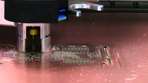
Hdi Pcba Manufacturer Laser technology
Laser technology is a multi-tasking technology introduced. It only uses a single ray of UV laser (CO2). It is used to build holes on the board.
Uses
It is used for
- Drilling
- Cutting
- Structuring
- Process VIAs
Q. Why Hdi Pcba Manufacturer use laser drilling in HDI?
HDI boards are small in size as compared to typical PCB. It is now a trend of miniaturization which means lessen the size of products. Therefore, Hdi Pcba Manufacturer uses micro vias that is why the laser system is used for drilling purposes in HDI.
Q. What is the size of micro vias used in HDI?
The VIAs used in HDI are of
Diameter less than 40 µm
Width less than 50 m
Q. What material Hdi Pcba Manufacturer uses in laser drilling?
A Laser beam uses resin-coated copper direct and forms blind VIAs on the board
The diameter of holes made; 30µm
A laser drilling machine can make 250 holes per second using copper.
Two head drilling machines can drill 1500-3000 holes on the board.
Finally, during the process, adhesive forms on the holes but after the copper layer has been drilled on the holes the resin/adhesive and fiberglass has been removed and VIAs are then plated.
Q. What is RCC?
Resin coated copper used by the drilling machine is RCC. Thin copper foils of about 5µm are used. And resins are about 50 µm thick.
Advantages
- Can be used for both rigid as well as flexible boards
- High yield properties
- Subsequently, it can be used for small-sized boards thus it can be used for HDI also.
- It can drill a hole as small as 0.075mm.
- An arc lamped pump laser can be used for convenience
- This lamp requires less cost and can work 300 hours. Moreover, takes less time.
Laser routing
According to Hdi Pcba Manufacturer, laser routing means forming curved edges on the surface of the board. It is done before punching tools and materials on the board.
It is done along the path where adhesive is used to avoid the leakage and squeezing out of the resin.
Similarly, Hdi Pcba Manufacturer uses UV rays for routing HDI boards.
Some additional materials used during laser routing/drilling of boards
- FR4
- Polyimide
- Epoxy resin
- Acrylate resin
- Solder masks
- Cover coats
- Galvano resists
Q. What is the cutting speed of laser routing?
According to the Hdi Pcba Manufacturer recommendation, the cutting speed without delaminating the board is 10 mm per second.
Advantage
After laser routing, there is no such need for cleaning the platform or the board again. Moreover, there is no need for any improvement later or before the fabrication.
HDI assembly
It somehow seems difficult to fit all the connections into a small area of PCB. But it is pointed by the Hdi Pcba Manufacturer that if a designer knows the hurdles while fitting the parts it would become easy to solve the issues.
- The testing of the HDI substrate is as easy as a typical substrate.
- Now 80% of the Multilayer Pcba manufacturers receive assembled flex circuits for HDI assembly from industries.
- HDI board needs almost 1005 components to be assembled.
Hdi Pcba Manufacturer driving forces
- Area array package
- VIA-inkpad
These two driving forces use for inquiry while testing and HDI assembly.
Testing
Many CAE/CAD software systems allow the testing for HDI assembly.
A built-in self-test (BIST) or boundary scan is used by many companies for testing. Moreover, Hdi Pcba Manufacturer designs their own circuits and uses the above-mentioned software for testing the limited access to the borders of the circuits.
Testing the board will cost about 30% of the total cost of the design that is why Design for Test DFT is the best way.
Q. Why Hdi Pcba Manufacturer test or verify the board?
Errors and failures of components while manufacturing PCB can be possible. That is why it is necessary for Hdi Pcba Manufacturer to verify the design. Design for Test DFT is the quickest way to diagnose and solve the problems.
What is DFT?
DFT stands for a design for the test. This term is used for testing the HDI assembly. Giving solutions to the problems during HDI assembly is design for test.
Planning before fabrication
A Multilayer Pcba Manufacturer must know all the basic fundamentals and information before proceeding. In addition, it is important to know the critical settings of the board to produce the exact yield you need.
A designer must have a plan before the otherwise continuous change in the board will increase the amount of use.
Q. How do Hdi Pcba Manufacturer plan before fabrication?
- Multilayer Pcba Manufacturer should know the count of layers and VIAsused in the board, this will help in the lamination process. As every layer and VIAs needs lamination so the counting before will tell you the accurate amount of lamination need.
- Usingstaged microvias will minimize the time as it does not need further copper filling.
- A Hdi Pcba Manufacturermust use trace space when needed.
- Control size of padswill also help to minimize the cost
Use of trace spaces in the board
- A Hdi Pcba Manufacturershould use trace spaces as needed for example around the fine pitch areas.
- But trace space can be used when the board is not as dense.
Q. What is the advantage of planning?
If a Multilayer Pcba Manufacturer plans the layouts and stacks before processing. It will be
- Easy to avoid errors
- Less time taking
- Minimize the budget
Post planning
All the functions and materials need a suitable condition, temperature as well as a platform.
After planning the board, a Multilayer Pcba Manufacturer should use a suitable place to complete the process.
Note; the board which takes more time will be less costly than the board which is completed in two days.
Surface finish
A Hdi Pcba Manufacturer can use the following surface finishes such as
- ENIG
- ENEPIG
- Hard gold
- soft gold
- immersion silver
- white tin
- HAL
- Lead-free HAL
Conclusion
HDI circuit boards are quite popular these days. These boards provide versatile modification and easy installation. With the help of hdi pcba manufacturer, you can put any electronic business on swift track. This technology has been somehow ruling over other circuits. It is growing day by day and becoming part of many devices.
