A comprehensive guide for China MCPCB Factory and Manufacturers and suppliers to avoid mcpcb issues in 2020
Table of contents - Shenzhen Mcpcb Factory
1. What will you learn from this article?
2. How does Shenzhen Mcpcb Factory Proceed PCB design?
3.Shenzhen Mcpcb Factory for Multilayer PCB
4.Drawbacks/difficulties/challenge
5.Shenzhen Mcpcb Factory Techniques and procedures
6.Types of multilayer PCB as recommended by Shenzhen Mcpcb Factory
7. How to be aware of moisture issues?
8.Ultra-multilayer PCB
9. How to be aware of thermal expansion?
10.Conclusion
What will you learn from this article?

Shenzhen Mcpcb Factory- Article will help you how to perform steps to design the PCB board in Shenzhen Mcpcb Factory. However, it is difficult to teach a PCB design, but it is good practice to start. Since mcpcb is a complex task, it is important to follow every instruction. Furthermore, you can learn all difficulties and challenges involved in building a perfect printed circuit board. In short, you will be learning from the gist of Mcpcb Manufacturers experience.
How does Shenzhen Mcpcb Factory Proceed pcb design?
China has been a major producer of small electronic equipment. And Shenzhen has a dominant space in it. Subsequently, it is also popular in making pcb designs for a number of electronics manufacturers. Therefore, these manufacturers belong to china and other countries. Similarly, there is a crowd of small units that produce minor and major components. Shenzhen Mcpcb Factory also exports this equipment. And earn huge revenue from it. Designing a printed circuit board is a major step. It involves particular skills.
After completing the design it’s time to turn the PCB on the board, for some designer’s PCB design is very easy and for some designers, this process is a very difficult task.
Even a specialist PCB designer may face some difficulties. Basically, there are departments of PCB design in many companies. While designing a board, the designer must have the knowledge of all connections, components, equipment used, tracks and all the manual tasks.
Important Note
Designing a board is an essential part however it is also hard for experiences designers as well.
Shenzhen Mcpcb Factory Components
Like any formal circuit traces of PCB also contain
- Capacitance
- Resistance
- Inductance
Such that the PCB design may face electrical and operational failure.
Q. Common applications of mcpcb
The printed circuit board is mainly used in the devices of computer
Such as
- Motherboard
- Network interface cards
- RAM chips
Q. What is the cause of PCB breakage?
Like all other circuits, PCB also has capacitance, resistance, and inductance which may low or high the speed or level of the circuit causing breakage.
Shenzhen Mcpcb Factory for Multilayer PCB
Q. What is a multilayer PCB?
Many layers placed over one another to form a PCB known as multilayer PCB. Similarly, it involves the interconnection of points and traces and makes a set of the layout.
Features
- Thin board
- Made up of with fiberglass
- Electric wires
Advantages
According to the leading Shenzhen Mcpcb Factory recommendations:
- Results of multilayer PCB is much better than a common PCB
- It follows a regular pattern of wiring
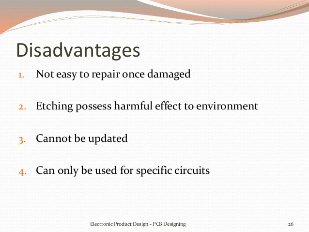
Drawbacks/difficulties/challenge
- It seems costly at the beginning of the process rather than that of the single-layer board
- It is difficult to repair a multilayer PCB because it has a complex network of traces and connections
- Moreover, it used high-quality equipment thus needs high temperature, because of the high temperature it causes expansion in instruments so this setup also needs a special surface.
- Simultaneously, making layers can become more difficult after another so it needs to pay more attention.
Shenzhen Mcpcb Factory Techniques and procedures
To complete the process, it involves different chemical processes to activate the wires and traces of layers.
Here are the steps of the procedure
- All the material and instruments like Drill, electrolytes, bits, copper plates must be available
- Make copper plates to initiate the procedure, it may be produced using different methods
- Shenzhen Mcpcb Factory Drill the holes using drill head to make holes and plate the holes with VIAs
- Clean the copper board
- Use acid of copper and electroplate the board
- Laminate the board
Shenzhen Mcpcb Factory also practice the following precautions
- Heat the layers to fuse signals and powers in the layout
- This will fuse the drills and plated layers first and then it’s time for lamination
- Why fusing the layers is important?
The multilayer PCB has a double number of layers (14 layers) and equipment than a PCB board (6-8 layers). Furthermore, it will make the whole process difficult and expensive as well. Fusing the layers will help to minimize the processes involve in the overall tasks.
VIAs
Signal VIAs; it makes the flow of signals through all the planes
Stitching VIAs; reduces the area, connected next to signal VIAs. It reduces the voice during cross-talks and noises produce.
Types of multilayer PCB as recommended by Shenzhen Mcpcb Factory
- Rigid multilayer PCB; uses costly instruments and expensive drilling heads thus it is high-cost PCB. It is a complex PCB.
- Flexible multilayer PCB; it has a flexible circuit and high-quality wires, it is a low-cost PCB. Subsequently, it is comparatively small in size.
Q. Which feature makes a PCB flexible?
Shenzhen Mcpcb Factory recommends using a smaller number of layers in a multilayer PCB that can make it flexible, as more layers will lessen the flexibility.
Note; in such a case a designer can make a high-quality PCB without facing these difficulties by
- knowing the basics of the process
- giving much time and attention to the process
- and by investing high cost
Quality
Due to fast generations, Shenzhen Mcpcb Factory high-speed quality equipment, instruments and semiconductors have been arisen. And these devices have a much greater quality of speed
E.g.
If we are using high-pin count in a device, there must be a high performing dielectric which will assist the increase in the speed of signals
Advantage

Using a high-speed digital in a circuit will increase the demand of the device, it also led the device to compete with other PCB devices in the market.
Problems
Highly cost material
Shenzhen Mcpcb Factory designer for its convenience selects a material that causes a small loss for dielectrics but that material may be costly purchased (does not meet the requirements).
In such cases the material which is lost Tangent causes difficulties while building.
(The things which are highly cost may not work worthy)
The products which are overprized are more difficult to handle and more challenging as compare to those materials
- which give poor results (yield)
- which does not meet the requirement of a designer
- or sometimes in worst cases impossible to build
Dielectric constant
- Moisture
Material when gets in contact with moisture it absorbs that moisture, moreover, it also absorbs the chemicals during the process.
Cause
Materials when absorbing the moisture with chemicals it disturbs the ratio of the Dielectric constant in a notable amount.
Q. How to be aware of moisture issues?
It is necessary to familiar with the following points:
- Select a material (Teflon/PTFE), which absorbs less moisture.
- Do not select material (ceramic substrate and polyimide), which absorb more moisture
- Temperature
The material which can change the performance due to temperature can also be problematic while the procedure. Therefore, Shenzhen Mcpcb Factory focuses on adequate temperature for mcpcb.
Cause
Changes in the value of DK due to irregular temperature can cause an effective change in the Dielectric constant.
It also causes a disturbance in fluctuation which is then difficult to handle.
Shenzhen Mcpcb Factory Ultra-multilayer PCB
Comparison
Typical PCB; 1.6 mm thick, 12 layers
Ultra-multilayer PCB; 6.3 mm thick, 80 layers
Resolving Technical issues
While making ultra-multilayer PCB there are some technical problems that occur and need to solve.
Laminating technology
Shenzhen Mcpcb Factory technology need high temperature and pressure and crush the layers to be laminated
The alignment of the drilling process and shields used in layers are reviewed.
Result;
- the shift of more than 150 µm lessen to 60 µm
- Now the spacing, connections, joining of holes and wires are avoidable
Properties
- Coefficient of thermal expansion
The temperature causes the expansion and variation of temperature to cause disturbance in the Dielectric constant during the process.
Q. How to be aware of thermal expansion?
The designer must have look at the expansion while building up the layers and aware of the mixing of material which have more expansion rate. This will help the design to be more proven.
- Thermal conductivity
Many Shenzhen Mcpcb Factory designs have a high-powered device; in such a case a stream of power generates throughout the design.
Cause
If the material has less thermal conductivity it will not bear the power generated and cause heat. Thus, a design must have good thermal conductivity.
- Dimensional stability
It is a property of multilayer PCB which will help the designer. Similarly, the material with less shrinkage property can make a good yield and cost high.
- Copper finish
This property is not noticeable. The smooth finish of copper can cause high frequency and high speed. It will boost the performance.
Effects
Contamination
A Shenzhen Mcpcb Factory PCB may contaminate by
- Flux residues
- Deposited salts
- Debris
Cause
This contamination causes leakage between the nodes of the board.
Even the board is clean enough you still see the contamination of about 10 nA.
Leakage
Even a small amount of contamination of about Nano ampere will cause an error in the output.
Example
10 nA contamination cause 0.1 V of error into a board with resistance 10 MΩ
Q. Will the neglectable amount of current injected in a node matter?
If the current is present at that time you can test it by providing fake moisture to the circuit. Shenzhen Mcpcb Factory blows moisture spots with a soda straw on the board. The moisture contacts with salt contents on the board, which may disturb the circuit.
Q. How to eliminate leakage problems?

Leakage problem can be eliminated by washing
Following are the steps:
- Wash the PCB first to remove the dust or particles
- Use isopropyl alcohol for brushing the board
- Use deionized water and thoroughly wash the board
- Bake the PCB at 85o for hours
- After the whole process of washing with solvents the residues highlight
Note; carefully use the solvents
Shenzhen Mcpcb Factory Design for PCB
After the Shenzhen Mcpcb Factory identification completes the next step is to divide PCB into portions with respect to the functions.
Proper use of power, ground, and signal planes are involved.
Separations; High-frequency circuits separated from low-frequency boards
Caution; handle the signal routing CAD and signal paths layout with care
Sequence of planes
- The Analog ground plane
- analog energy plane
- Digital surface plane
- The digital power plane
Note; not any plane should overlap
Conclusion
- Be aware of Dielectric constant and loss Tangent
- All the above knowledge will help the fabrication easy and less costly
- Ultra-multilayer PCB lead to more difficulties
- It will succeed the designers, engineers, suppliers, consumers to make the final product.
- Must know the basic steps of the process
- The above knowledge will assist to make a good PCB with more yield in a manageable cost
