Everything You Need to Know about PCB Board manufacturing
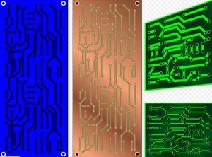
After separating electronic device, you will be able to find a Printed circuit board. Its appearance is like a small green board that is composed of marking on it. In short we will say that it’s like a maze. Before diving into the main guide to PCB Board manufacturing process, first we want to put shed to the main definition of printed circuit board for better understanding.
Printed Circuit Board Overview
Small green boards in the electronic application plays an important role in the complete functioning of a device. If you cut them out from device, your application will be useless. Printed Circuit Board works like a backbone of all modern electrical applications. If you are going to make such device that will perform some computation then PCB must be inside it. Here we are giving you an example for better understanding. If you explore the digital clock it must have a small printed circuit board inside it. Though the digital clock is a simpler item but it still has. Our electronic industry is surrounding with PCB, it’s like a base to any device.
Printed Circuit Board actually transfer signals to the device for performing action. Though the Printed Circuit Boards are small but PCB Board manufacturing process can be vast.
If you are one those who want to make its own PCB then you have to follow multiple steps. Let’s continue to read below and know everything in detailed about PCB Board manufacturing process. This guide wills definitely going to help you in making a good Printed Circuit Board for yourself.
PCB Board manufacturing Process – Step by Step Guide
Most commonly element used by printed circuit board is copper. First of all copper is laminated to substrate and it for exposing the designing of Printed circuit board it is curved away.
A printed Circuit Board is composed of multiple layers in a line altogether. They are bonded together in order to fit them securely so let’s get in to the guide with us.
Design
Design is one of the main important factors in the PCB Board manufacturing process. You can complete the designing process via computer software. Commonly trace width calculator is used for getting details of inner and external layer.
Design Printing
After making design, the second important thing is printing. In order to print the design of printed circuit board you have to use a Plotted Printer. Plotted Printer plays an important role in creating film that shows the layers of PCB briefly. While printing process two colors are used on the inside layer, first one is clear ink which is used to show that nonconductive areas second one is black ink which is used to show the copper conductive traces.
Creating Substrate
The 3rd step is to create a substrate; it is an insulating material combination of epoxy resin & glass fiber.
While forming PCB, substrate holds the components on the structure; the material is passes by oven.
Here copper is laminated on the both sides of layer and etched away in order to show the design from printed film.
Inner layer Printing
In this step a photo sensitive film will get to harden by exposing it to ultra violet light in order to cover the structure. Photo sensitive film is actually come into being by the combination of photo reactive chemical. This photo sensitive film actually plays an important role in aligning the blueprints and actual prints of printed circuit board. For alignment process you need to be drilled holes in to the printed circuit board.
Ultraviolet Light
In the 5th step you have to pass the laminate and resist from ultra violet light. Doing this will harden the photo resist. This ultra violet light plays an important role in revealing the pathways of copper. Later on we recommend you to remove the black ink; it will prevent the areas from hardening. After confirming that the board is now hardened, wash it via alanine water in order to wipe out excessive photo resist.
Remove unwanted copper
In the 6th step you have to wipe out the unwanted copper by using solution similar to alkaline. Keep in mind that the hardened photo resist remains intact while removing copper.
Inspection
7th thing that you have to do is to inspect the newly cleaned layer for alignments. The holes that you drilled in the earliest steps will keep the alignment of inner and outer layer. In order to drill pins via holes use an optical punch machine and then make use of inspection machine in order to ensure no errors. After this step, you cannot remove any errors, so dive into next steps carefully.
Layers Lamination
In this step, you will be finally able to see that PCB has been taken a shape, all the layers has been merged together. Before starting laminating process, you can see clearly that metal clamps are the one that holding layers altogether. Prepreg (epoxy resin) is above the alignment base. Layer of substrate goes over the Prepreg. At the end, no more copper layer is applied which is press plate.
Layers Pressing
In the 9th step, in order to press all the layers mechanical press is used. In order aligned and secure the layers, at the end pins are punched. You can also remove the pins at the end incase if you are using a modern technology. After following above instructions you have to send the PCB to the laminating press. It will provide heat and pressure; more heat will melt the epoxy inside the prepreg which becomes the reason of layers fusion.
Drilling
In the 10th step, you have to drill the holes in layers. This drilling will expose the substrate an inner layer. More unwanted copper will also be removed in this step.
Plating
Finally it’s a time to plate the board; you have to clean it by a chemical solution. After applying chemical for fusing layers, now you can wipe it by applying another chemical.
Outer Layer Imaging
In 12th step you have applied photoresist to the outer layer same as we did in the 3rd step.
Plating
This step is similar like step 11; you have plated the panel via copper layer and then layered a thin guard to a board.
Etching
In this step PCB connections are established by using chemical solution for removing unwanted copper.
Solder Mask Application
Finally it’s a time to apply solder mask but before applying you have to wipe out the panels. Epoxy is also applied along solder mask. Solder mask is actually giving green color to the printed circuit board. You can remove the unwanted solder mask by passing ultra violet light. As we all know very well that excess in anything can be bad.
Silk-screening
In the sixteen steps, you have to do silk screening. It is one of the most important steps to consider. In this process critical information is printed on to the board. This critical information can be letters or numbers; it will actually help the user for using it easily. After silk screening you have to apply last coating and pass printed circuit board via curing process.
Surface Finishing
This is almost the last step, finally you have to plate the PCB via solder able polish, it will play an important role in increasing the quality of solder.
Testing
Its end, now you have to pass it to the technician for testing purpose. If he says that it’s working fine then use it in the electronic device.
Bottom Line
As we all knows PCB Board manufacturing process is not really easy, it requires very lengthy steps, time, effort and material. If you think you can manage all these things then start this PCB Board manufacturing process. Otherwise it will be good for you to hire good PCB Board manufacturers.
HUAFENG, offers high quality prototypes and fast-rotating printed circuit boards (PCBs).
Contact at (+86) 0755-83388898, you can also leave an email at melinda@hfdspcb.com.
HUAFENG is a well-known reputable worldwide company offering quality prototypes and fast-rotating printed circuit boards all around the world. Our engineers are serving us since decades. We give only warranted services so don you worry about product quality. You will never regret by spending your hard earned money on us. We have been awarded by multiple international certifications for producing high quality Printed Circuit Board, so you can trust us without hesitation.
This article reviews the Boiled Egg Diet and whether it's effective. cialis online It can be frustrating trying to get rid of upper pubic fat.
