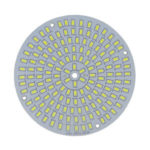
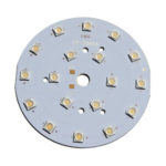
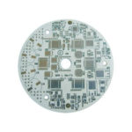


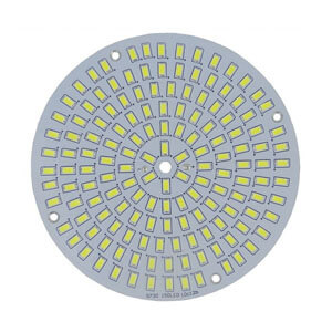
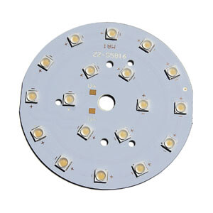
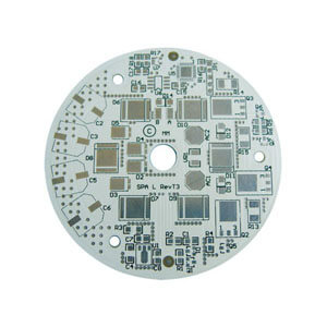
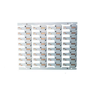

Aluminum PCBs are printed Circuit Boards that contain a thin layer of conductive dielectric material. They are also known as Aluminum Clad, Aluminum base, MCPCB (Metal Clad Printed Circuit Board), IMS (Insulated Metal Substrate), Thermally Conductive PCBs, etc. Aluminum PCBs were developed in the 1970s, soon after which they’re applications increased dramatically. The first application was their use in Amplification Hybrid Integrated Circuits.
The basic structure of Aluminum PCBs is four layered. It consists of a layer of copper foil, a dielectric layer, an aluminum base layer, and an aluminum base membrane.
Specification:
| Layers | 1-2 layers |
| Material | Aluminum, Copper |
| Production Capacity | 7000㎡/months |
| Board shape | Rectangular, Round, Slots, Cutouts, Complex Irregular |
| Min Board size | 5mm*5mm |
| Max Board size | 1500mm*1500mm |
| Min Tracing/Spacing | 0.1mm |
| Board thickness | 0.3mm-5.0mm |
| Copper thickness | 1oz-10oz |
| Dimensional tolerance | ±0.15mm(Die blank); +-0.10mm(CNC) |
| V-CUT tolerance | ±0.1mm |
| Hole tolerance | ±0.076mm |
Application:
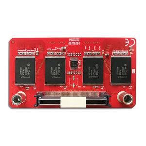
PCB is mainly used in automotive electronics, industrial control power supply, IT communication, medical equipment, etc., and is committed to becoming the best quality value-added service solution provider for small and medium batches and allegro production.
Deliverability:
| Layers | m² | Deliverability | m² | Deliverability |
| 2L | <1m² | 5 days | <3m² | 5 days |
| 4L | <1m² | 6 days | <3m² | 7 days |
| 6L | <1m² | 8 days | <3m² | 9 days |
| 8L | <1m² | 8 days | <3m² | 9 days |
Notes:
The standard plate is ordinary FR-4 Tg130 without a specified brand.
Minimum line width/space: 4MIL.
Inner/outer finish copper thickness: 35/35um.
Minimum aperture: 0.30MM.
Surface treatment process: lead spray, lead-free spray, OSP.