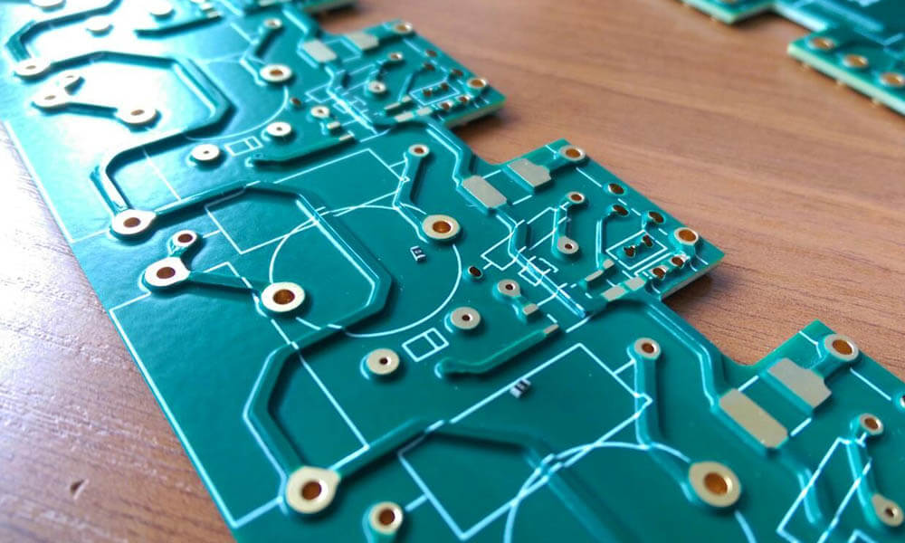
Thick copper usually means the copper foil thickness of PCB higher than 3 ounces (4 mils or 100 microns). It mostly used for high power (electric current) electronics like a power supply or some power circuit in the automotive industry. It can be designed in the inner layer or outer layer. In PCB production, it is more difficult than traditional circuits with copper foil less than 2 ounces.
Heavy Copper PCB Capabilities:
- Maximum Number of Layers = 32
- Laminate – FR-4 (All Tg Ranges), Teflon, Ceramic, Metal Core
- Finished Thickness = .020″ – .275″
- Green, Blue, Red, Black, Clear & White Solder Masks & Legend Inks
- Minimum Soldermask Clearance – 6 mils
- Minimum Solder Dam Width – 5.5 mils
- Hot Air Solder Leveling (HASL)
- Immersion Gold (ENIG) & Immersion Silver
- Blind & Buried Vias
- Minimum Drill Bit Hole Size = .012″
- Minimum Holes Size – .008″ +.005″/-.008″
- Maximum Hole Aspect Ratio = 30:1
- Maximum Copper Weight = 30 oz.
- Controlled Impedance +/- 10%
- Minimum Silkscreen Line Width – 8 mils
Etching of pattern is one of the major issues need to overcome for thick copper PCB. When the copper thickness becomes thicker, the etching process time will be longer. When the etching solution removes the copper vertically, it will also cause side etching simultaneously. Finally, the pattern will have a big “foot” which has a much smaller width on the top than on the bottom. It always reduces the copper volume used to transfer current. To meet the design criteria, the PCB fabricator needs to make trace width compensation first so that the line width can pass the specification. It means a wider trace space is also important. When the copper thickness higher than 5 ounces, the problem becomes more difficult. The thicker the copper foil, the wider the design trace/space width is a common perception.
The second process to be concerned is lamination. To fill the space being etched off, it needs a lot of resin to fill in. Usually, the resin needs to come from the prepreg. So the PCB fabricator is always used multiple high resin content prepreg in heavy copper construction. However, it will cause many problems.
1. The total thickness will become high. If the prepreg used is too less, it may cause the void inside. But too many prepregs may cause the total thickness or dielectric thickness between layer out of specification.
2. During lamination, the multiple high resin content prepreg will have high resin flow and cause the inner layer shift. The layer-to-layer misregistration will become a problem for the fabricator to overcome.
3. The resin-rich area may have resin crack issues for its no reinforcement. The higher CTE also cause some reliability issue in higher temperature.
The third issue needs to be concerned is the drilling. When the design has many thick coppers, the drilling parameter needs to adjust to more similar to drill a thick copper plate. The drill bit wear and debris removal need to be processed carefully.
The fourth problem is on the solder mask process. It’s difficult to apply enough solder mask to cover thick copper pattern and base material with severe height difference. Usually, the manufacturer needs to fill more solder masks to fill in the space between the trace. It’s common to apply multiple printing. The first printing fills most of the pattern gap and second printing cover enough thick of solder mask on the trace pattern. But it still has some risk of voiding. The thick solder mask is also more difficult to expose and develop. If the exposure energy is too weak, then some undercut problems may happen.
One issue that the power supply designer looked at is the high potential test (Hi-Pot Test). To get enough insulation to resist high voltage testing, the material, multilayer stack-up, inner layer cleanness, etching, and design are all important. Sometimes the drilling, routing, and plating also play an important role to get good electrical insulation.
When the copper thickness goes even higher like 10 ounces or higher, the manufacturing process needs to make some change. The manufacturer can apply some resin on the trace gap first to prevent too much resin filling or the risk of voiding. This is also the key to manufacture multiple thick copper pattern on one layer.
Applications that require running a high power we offer heavy and extreme copper tracing, plated through holes (PTH), surface pads and ground planes. By electroplating heavier copper to your PCB you are ensuring high reliability and efficient power distribution. In fact, we have found that heavy copper tracing can even act as its own heat exchanger dissipating as much as 20% of overall temperature. Extreme copper thickness can be plated as high as 30oz.
PCB applications:
- High Power Distribution
- Planar Transformers
- Heat Dissipation
- Power Converters
- Amplification Systems
- Solar Panel Manufactures
- Power Controllers
- Welding Equipment
