Every PCB Designer must have to Know Design Guideline - PCB Made in China
If you are one of those who want to made a perfect Printed Circuit Board and don’t want to face delays and unnecessary cost then we recommends you highly to have a look upon these design guidelines – PCB made in China. These guidelines will definitely going to help you in making a extra ordinary PCB.
Top Design Guidelines for Engineers – PCB Made in China
There are many designers that took the designing step not seriously, so at the end they always comes up with some faults that can create lot of troubles for the manufacturers. So we recommend all of the designers highly that don’t take the designing step for granted and give you’re a bit time in focusing designing PCB.
Here we are going to share the key that will help you in designing a board so let’s explore it.
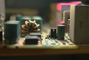
Fine Tuning your Component Placement
This step is like an art or science; it requires a strong focus about the prime real estate available on the board. If you are unintentionally placing PCB components down to vias then definitely there are chances of affecting performance.
This process is a bit difficult especially for newbies; you have to place the electronic components in right way because this way of placing component will help you to know that how easy or difficult will be to manufacture a board. Component placement will also differentiate that does it meet your original PCB design or not.
Though there are many rules for electronic component placement but here we are going to put shed on the main ones that will definitely going to help you.
Orientation:
Make sure to place same components in the same direction, this will play an important role in effective routing. Doing this will also plays an important role in error free and efficient soldering process during assembly.
Placement:
Another thing to keep in minds that do not place the electronic components on the solder side of board.
Organization:
We recommend you highly to place all SMD on the same side, for this you can follow SMD PCB Design rules. Another thing that you have to do is to place TH components on the top side of the board, if you follow this then number of assembly steps will be reduced.
Also keep in mind that when designer make use of mixed technology then you have to add more steps for assembly, doing this will not only take your time and effort but will be costly also.
#2: Placing Your Power, Ground & Signal Trace
Orienting Power and Ground Planes
Make sure to have power and ground planes internal, symmetrical and centered to PCB. Doing this will plays an important role in preventing the board from bending.
Note: this step is not necessary incase if you have 2-layer boards. In order to power ICs we recommend you to use common rails, also make sure that you have solid and wide traces.
Routing Guidelines for PCB Layouts
Now you have to connect signal traces for matching schematic guidelines. We recommend you to place traces as shortly and directly as possible b/w components. If your component placement forces you to trace router horizontally on one side of board then we recommend you highly to route traces vertically on opposite side of board.
The rules will become more complex because the number of layers is increasing.
Defining Net Widths
Now you have to define the net widths, we recommend you to provide a 0.010” width for low current analog and digital signals. Also make sure that PCB traces that carry more than 0.3 A must be wider.
#3 - Keeping Things Separate
In order to minimize the voltage interference issue, you can follow below steps.
Separation:
We recommend you strongly to keep separate the power and control ground. If it’s necessary to tie both then we recommend you to keep it at the end of your supply path.
Placement:
Incase if you have placed ground plane in the middle layer then we will recommend you to keep a short impedance path. Doing this will keep the board safe from any power interference. Following this strategy will also plays an important role in controlling the signals.
Coupling:
We will recommend you to have your analog ground crossed only by analog line, doing this will reduce the capacitive coupling.
#4 - Combating Heating Issues
As we all knows that almost 50% boards damages because of heat issues, designers don’t take it seriously but this issue can affect the designers badly when they are not taking heat dissipation strategies seriously.
Identifying Troublesome Components
First step is to find out the part that is responsible for creating more heat. After finding that component, you have to add heat sinks and cooling fan, this will plays an important role in keeping the temperature down. Also make sure to keep away the critical parts from high heat producing component.
If your board in such a situation that it’s 2 or more components is generating high heat then we recommend you strongly to distribute these parts from board. Doing this will keep the board safe from producing a hot spot.
Adding Thermal Reliefs
Now you have to add a thermal relief, we recommend it highly to add it because it will make the soldering process as easy as possible. Doing this also plays an important role in slowing the rate of heat sinking.
Moreover you can also add teardrops; this will plays an important role in join traces with pads in order to provide more metal support.
This will also be the reason of reducing mechanical and thermal stress.
#5 - Checking Your Layout against Your PCB Design Rules – PCB made in China
Last but not least, you have double or triple check your work in order to remove any error. This step will actually clear out the thing whether you are successful or not.
We recommend you to start with ERC and DRC in order to verify whether you have met all the rules or not. ERC and DRC will help you to define the gap b/w traces, width common manufacturing requirements, high-speed electrical requirements, and other physical requirements for the device.
Note: Many design process comes up with a statement that you would better to check run design rule checks at the end of the design phase. But if you have chosen a right designing tool then you can run checks throughout the design process.
Appropriate tool will help you to define the designing potential issues, and you will keep correcting side by side.
Well! If you have achieved your ERC and DRC error free output, then we recommend you to double check the routing of every signal. Also make sure that you have not missed anything by running through your schematic one wire at a time.
At the end also make sure that PCB layout is matched with schematic by utilizing design tools probing & masking feature.
Conclusion:
The short conclusion of this Article is that we ended up sharing the top 5 PCB Design Guideline – PCB Made in China that every PCB manufacturer must have to read it. If you follow the above list wisely then we are damn sure that at the end the results will be outstanding. You will be able to produce quality Printed circuit board. Hope these practices will be helpful for you, if you liked this Article then share it with others.
Also stay tuned with us because many more information are coming soon. If you are one of those who is looking for high quality and valuable PCB made in China, then you are at the right place.
HUAFENG, is offering high-quality prototypes and fast-rotating printed circuit boards (PCBs). We are a reputable and quickly growing company. HUAFENG only offers quality and warranted services, our engineers have been serving us since decade. They are specialized in producing electronic circuit board for communications, medical, industrial and automotive devices so you can rely on us. We assure you that our product performance and durability will be extra ordinary.
If you want to know more about us then you can make a call at (+86) 0755-83388898, you can also leave an email at melinda@hfdspcb.com. Our support team is very responsive they will reply your each question briefly.
En revanche, vous vous mettez en danger si vous achetez du viagra contrefait en ligne, sans avoir une ordonnance. Le Viagra agit en arrêtant le processus chimique qui permet au sang de quitter votre pénis en érection. casino canada Voici quelques astuces pour rendre le viagra plus efficace.
