Double-Sided PCB Manufacturing: The Step by Step Guide
The processing need for sophisticated electronics can only be filled via Double-sided PCB manufacturing. It seems that double-sided PCB is the gateway to higher innovative applications. They focus on efficiency and effectiveness.
Due to numerous advantages of Double-Sided Printed Circuit Boards, they have become the mainstream PCBs for all businesses across the globe. What more is that you can even enjoy customized Double-Sided PCB Manufacturing.
Customized PCB helps you design and develop Printed Circuit Boards that are according to your product requirement. Thus, ensuring the quality and efficiency of the product. To choose the right kind of Printed Circuit Board, it is important to have a basic understanding of its manufacturing process.
In case you are not familiar with the manufacturing process of double-sided PCB, we will rectify that for you. Here, we will provide you with a concise guide one double-sided Printed Circuit Board manufacturing process.
The Complete Guide on the Manufacturing Process
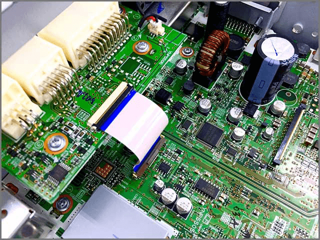
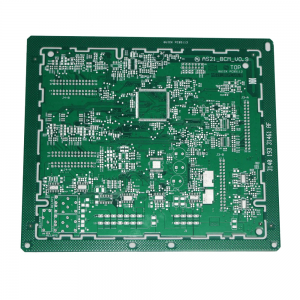
Double-sided Printed Circuit Boards use both the bottom as well as the top layers with vias to offer different routing traces. Manufacturers today use a number of materials as a PCB substrate. Different materials offer different benefits.
For instance, for a basic electronic, a good idea is to use FR4 as the base substrate. In addition to being reasonable, it offers a certain degree of stability under changing temperature conditions. Another great thing about FR4 is that is not easily breakable.
FR4 is an excellent choice for affordable commercial products. However, for designs that require high performance, using PTEF base circuit printed boards would be a wise option.
To make the component tracks of a Printed Circuit board, you first need to obtain a copper clad board. The board generally comprises of FR4 as the substrate material with both sides of copper cladding. The copper cladding consists of a copper sheet. This sheet is extremely thin and is bounded to the board.
Although, bounding works well with FR4, however, it can be trouble for PTFE. It tends to make the processing of PTFE Printed Circuit Board a bit challenging.
Substrate
The first step is needing a substrate. In general, the manufacturer uses fiberglass to make the substrate. The reason they use fiberglass is that it offers robustness. It tends to provide core strength to Printed Circuit Boards.
In addition, it stands against breakage. To make your life easy, we label the substrate as the skeleton of the Printed Circuit Board.
Copper Layer
Manufacturers can either use a full-on copper or a copper foil for this particular layer. The type they use greatly depends upon the board requirement and type. No matter the approach they use, the primary purpose of the copper layer remains the same i.e. to transmit the electrical signals in an effective manner.
They would carry these electrical signals to and forth the Printed Circuit Board.
Solder Mask
Next in line of the double-sided PCB manufacturing is solder masking. This layer which usually is of Polymer assists in copper protection. It ensures that in case if the circuit comes into contact with the environment, there is no short-circuiting.
In other words, we can say that the solder mask is basically the skin of the Printed Circuit Board.
Silkscreen
The silkscreen is final, yet an important part of the Printed Circuit Boards. The manufacturers place silkscreen on the component side of the Printed Board. It shows logos, numbers, settings of symbols switch among others.
Now that you have an idea of the basic steps, let go a bit more detail of the customized PCB Manufacturing Process.
Photo plots
A good manufacturer starts the manufacturing process by creating plots. They use data given by the customer to create these photo plots. You use the customer’s PCB style to gather the Gerber data. For instance, the Focus on, Protel, Eagle, etc.
Cam-Bearbeitung
You would need the information to form several software solutions. You then back them up in an Ext. Gerber File format. You can use the Ext. Gerber structure file as the preview of the Printed Circuit Board.
Manufacturing Flow Process
Preparation
First, you need to prepare the material. Drill entry materials along with the copper-clad panels are kept at hand. There is about 1.6mm of the solid base material in a standard panel. It covers around 18 µm copper on every side.
Drilling and Pinning
After drilling the tolling tools, it is time to move the next step. The manufacturers would not pin the PCB panel onto the CNC machine.
Printed Circuit Board CNC Drilling
Double-sided PCB manufacturing drilling technique is different from single-sided Printed Circuit Boards. They generally use the through-hole technique. However, it is possible to choose other techniques as well.
They create component drills as well as the through-hole plated using a CNC drill device.
Through-hole plating
An electrographic film such as the Palladium is effectively electroplated to the drill cavity’s wall structure. Of course, you can use another type of electrographic film. However, Palladium is the most common one.
Attaching the electrographic films allow the galvanization of copper at the later stages of the manufacturing process.
Brushing
It is imperative for the Printed Circuit Board to be completely clear of any sort of dirt or grease. Therefore, they need to be thoroughly cleaned before heading out to the next stage of the double-sided PCB manufacturing process.
A good technique for cleaning the Printed Circuit Board is brushing.
Laminating
Laminating is another important part of the manufacturing process. To laminate the PCB panel, you would require extreme temperature as well as pressure.
Resist Exposure
You should use the photo plots to ensure resists against the UV light.
Development
When the PCB creates about 1% of the sodium carbonate via the cycling building, it means that the PCB is actually ready for the plating.
Electroplated Configuration
Pads and tracks are copper plated to the board. They generally have a thickness of around 35 µm. To fuse it, they use a tin film of 6 µm to 10 µm. Doing this helps them safeguard the tracks and the pads during the final etching process.
Resist Stripping
2.5% of caustic potash answer asides with the photoresist. This leads to the spray and immersion coating process.
Etching
Next is the spraying of ammonia onto the copper film. The manufacturer would give an ammonia coating. This helps is eliminating unwanted copper.
Tin Stripping
To remove the tin you would need a nitric acid. The tin-stripper than leads to the spraying and dipping procedures.
Solder mask Applications
Now, you have to apply the solder mask. After this, comes the spraying as well as the screen-printing procedure.
Exposure
Lastly, the solder mask is exposed to the sunlight. The double-sided PCB manufacturing process would use photo plots.
Silkscreen
The silkscreen is imprinted onto the solder mask. It provides all the basic labeling of
Surface finish
For the surface finish, they use the chemical nickel gold along with vertical baths. To ensure solderability, the manufacturer does the gold coating on the nickel surface.
 Take Away
 Take Away
Now that you have a basic understanding of the double-sided PCB manufacturing process, you will be able to make a more learned decision in terms of PCB type and manufacturer.
CCTC-HFTC is among the leading PCB manufacturers. They are years of experience and highly knowledgeable staff to ensure the highest quality of Printed Circuit Boards within the required time frame.
