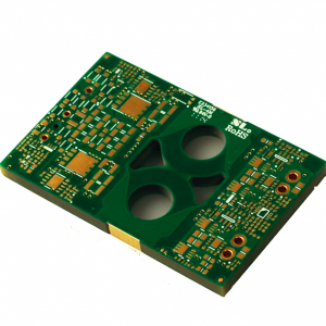


PCB Capability
|
PCB capability
|
|||
|
Item
|
PCB capability
|
PCB capability
|
PCB capability
|
|
Max Layer
|
60L
|
8L
|
36L
|
|
Inner Layer Min Trace/Space
|
3/3mil
|
3/3mil
|
3/3mil
|
|
Out Layer Min Trace/Space
|
3/3mll
|
3.5/4mll
|
3.5/4mll
|
|
Inner Layer Max Copper
|
6oz
|
2oz
|
6oz
|
|
Out Layer Max Copper
|
6oz
|
2oz
|
3oz
|
|
Min Mechanical Driling
|
0.15mm
|
0.1mm
|
0.15mm
|
|
Min Laser Drilling
|
0.1mm
|
0.1mm
|
0.1mm
|
|
Max Aspect Ratio(Mechanical Driling)
|
20:01
|
10:01
|
12:01
|
|
Max Aspect Ratio(Laser Drilling)
|
1:01
|
/
|
1:01
|
|
Press Fit Hole Ttolerance
|
±0.05mm
|
±0.05mm
|
±0.05mm
|
|
PTH Tolerance
|
±0.075mm
|
±0.075mm
|
±0.075mm
|
|
NPTH Tolerance
|
±0.05mm
|
±0.05mm
|
±0.05mm
|
|
Countersink Tolerance
|
±0.15mm
|
±0.15mm
|
±0.15mm
|
|
Board Thickness
|
0.4-8mm
|
0.1-0.5mm
|
0.4-3mm
|
|
Board Thickness Tolerance(<1.0mm)
|
±0.1mm
|
±0.05mm
|
±0.1mm
|
|
Board Thickness Tolerance(≥1.0mm)
|
±10%
|
/
|
±10%
|
|
Min Board Size
|
10*10mm
|
5*10 mm
|
10*10mm
|
|
Max Board Slze
|
22.5*30 inch
|
9*14 inch
|
22.5*30 inch
|
|
Contour Tolerance
|
±0.1mm
|
±0.05mm
|
±0.1mm
|
|
Min BGA
|
7mil
|
7mil
|
7mil
|
|
Min SMT
|
7*10mil
|
7*10mll
|
7*10mll
|
|
Min Solder Mask Clearance
|
1.5mil
|
3mil
|
1.5mil
|
|
Min Solder Mask Dam
|
3mil
|
8mil
|
3mil
|
|
Min Legend Width/Height
|
4/23mil
|
4/23mil
|
4/23mil
|
|
Strain Fillet Width
|
/
|
1.5±0.5mm
|
1.5±0.5mm
|
|
Bow &Twist
|
0.003
|
/
|
0.0005
|
|
PCB Lead Time
|
||
|
Layer
|
Quick Turn/ Usual Time
|
Mass Production
|
|
2L
|
24hours /4 days
|
8-10 days
|
|
4L
|
48hours /5 days
|
10-12 days
|
|
6L
|
72hours /6 days
|
12-14 days
|
|
8L
|
72hours /7 days
|
16-18 days
|
|
10L
|
96hours /8 days
|
18-20 days
|
|
≥12L
|
96hours /10 days
|
18-20 days
|