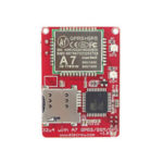
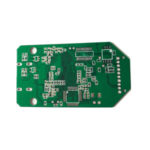
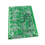
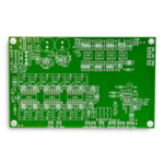
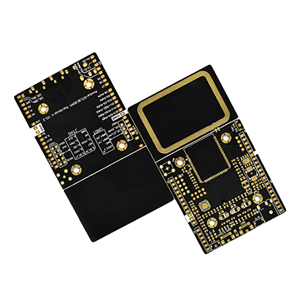
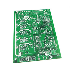
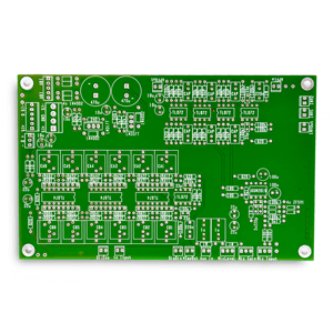
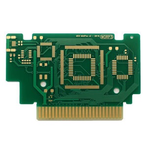
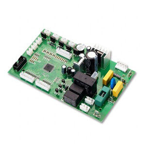
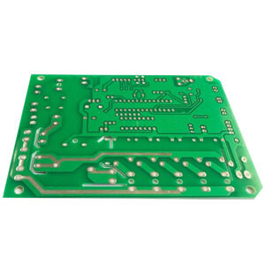
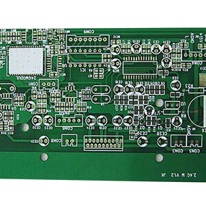
We are offering a high-quality range of printed ceramics thick film circuit substrate PCB to our most reliable clients. These products are widely used in various applications. The offered range of products is made from optimum quality material and manufactured under the supervision of an expert team of professionals. In order to ensure quality, the entire range is rigorously tested against various quality parameters by our quality controllers. Keeping in mind the diverse requirements of our clients, we provide the entire range in various sizes and specifications and at affordable prices.
Specification:
| Number of Layers | 10 layers |
| Base Material | FR-4/aluminum/ceramic/cem-3/FR-1 |
| Board thickness | 1.6mm |
| Copper Thickness | 1oz |
| Min. Hole Size | 0.1mm |
| Min. Line Width | 3mil |
| Min. Line Spacing | 3mil |
| Surface Finishing | Lead-Free HASL/ENIG/Gold Finger/OSP |
| Solder Mask | Green/Black/White/Red/Blue/Customized |
| Testing Service | 100% E-testing |
Application:
PCB is mainly used in automotive electronics, industrial control power supply, IT communication, medical equipment, etc., and is committed to becoming the best quality value-added service solution provider for small and medium batches and allegro production.
Deliverability:
| Layers | m² | Deliverability | m² | Deliverability |
| 2L | <1m² | 5 days | <3m² | 5 days |
| 4L | <1m² | 6 days | <3m² | 7 days |
| 6L | <1m² | 8 days | <3m² | 9 days |
| 8L | <1m² | 8 days | <3m² | 9 days |
Notes:
The standard plate is ordinary FR-4 Tg130 without a specified brand.
Minimum line width/space: 4MIL.
Inner/outer finish copper thickness: 35/35um.
Minimum aperture: 0.30MM.
Surface treatment process: lead spray, lead-free spray, OSP.


