General Design Considerations
The general parameters to be considered before and during the design of any printed circuit board, but focuses on boards incorporating copper weights ≥ 3oz/ft2. The following parameters can and will have a major impact on reliability and performance of the end product. Founded believes the parameters listed in this section are a MINIMUM to be considered. A comprehensive listing of all parameters and their design/performance tradeoffs is shown in IPC-2221.
End-Product Requirements
The end product requirements must be known before design start-up. Servicing and maintenance of the end product can directly influence conductor routing, part placement, board size, markings, coatings and final finish.
Performance Considerations
Finished printed circuit boards manufactured by Founded meet or exceed the performance requirements of IPC-6011. There are three general end product performance classes that IPC-6011 has established. Class 1 is "general electronic products", Class 2 is "dedicated service electronic products" and Class 3 is "high reliability electronic products". Please see IPC-6011 or IPC-2221 for more information on the 3 classes. Founded requires all products to be class specified and any exceptions or additions to the specifications to be clearly indicated on the master drawings.
Material Type & Properties
There are several material choices available to the designer, ranging from standard printed circuit board epoxy resins to advanced dielectrics with specialized properties. There are a number of properties the designer must consider, including but not limited to; temperature (soldering and operating), electrical properties, structural strength, flame resistance, machine ability, CTE, thermal conductivity and thermal stability. Laminate materials should be selected from materials listed in IPC-4101.
It is important to note that for high current designs the temperature rise due to current flow in the conductor, when added to all other sources of heat at the conductor/laminate interface, do not exceed the maximum operating temperature specified for the laminate or the assembly. See IPC-2222 for maximum operating temperature for laminate materials. Materials used (prepreg, copper-clad, copper foil, heatsink, etc.) and minimum dielectric thickness/spacing must be specified on the master drawing.
Markings, Coatings & Final Finish
Solder mask is used to provide a hard, durable solder resistant coating that also has electrical insulation properties. Founded applies solder mask coatings in accordance with IPC-SM-840. Solder mask can be used to protect (tent) vias from process solutions and soldering. The maximum finished hole diameter that can effectively be tented is 0.025". Larger hole diameter tenting must be agreed to between the end user and Founded. The electrical insulation properties of solder mask depend on the thickness applied and the type of mask used.
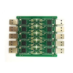
EXTREME Copper PCBEXTREME Copper Circuit Boards
Founded has developed a "capping" process that provides greater electrical insulation properties than regular solder mask. This process involves bonding a thin layer of epoxy resin to specified areas of the completed printed circuit board. Designers must specify how much insulation is required and where the "cap" is to be placed. Please note that surfaces under the "cap" will not be available for soldering.
All markings and/or legends required by the end user must be specified on the master drawings. The type of marking (non-conductive ink, etched characters, or other methods) must be clearly specified. Markings should be placed to avoid being covered by components and should never be on conductive surfaces. Whenever practical, part number, revision, layer number and orientation markings should be incorporated on the master artwork. Most non-conductive inks are liquid screened and markings within 0.020" MAY be slipped 0.005" or more from solderable surface. Please note that liquid screened marking's legibility is affected by high surface irregularities.
Test specimens (coupons) are used as representatives of the printed circuit boards fabricated on the same panel. Coupons are used for most destructive quality evaluations and evaluations that require a specific design that doesn't exist on the printed circuit board. Founded evaluation purposes. Layer to layer registration, copper thickness on each layer and in plated through holes, plating adhesion, solderability, soldermask thickness and soldermask adhesion are some of the process parameters evaluated. Material quality assurance is based on statistical sampling norm