n PCB design, when PCB mass production is finally carried out, PCB assembly is also a very important thing. This not only involves the quality standards of PCB circuit boards, but also affects the cost of PCB production. How to make a reasonable and effective jigsaw on the premise of ensuring the quality of the PCB circuit board, thereby saving raw materials, is a problem that production companies pay great attention to.
1, imposition connection
PCB imposition linking method There are two linking methods, one is V-cut (as shown in Figure 1-1), and the other is the stamp hole linking method (as shown in Figure 1-2).
V-cut is generally suitable for PCBs with a rectangular shape, which is characterized by neat edges and low processing costs after separation. It is recommended to use them as shown in Figure 1-3.

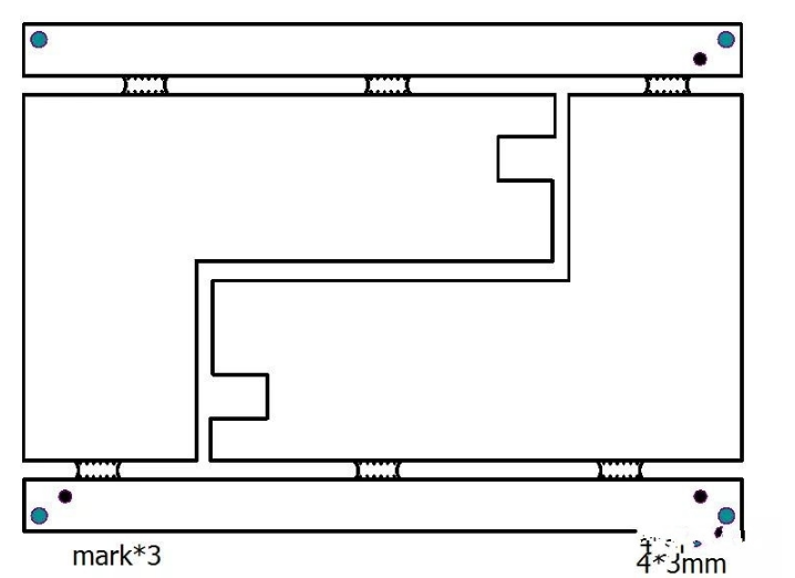
Stamp holes are generally suitable for irregular layout imposition. For example, the “L” -shaped plate and frame structure of MID often uses the stamp hole linking method for imposition, as shown in Figure 1-4;
2. Number of impositions:
The size of the entire imposition must be calculated according to the size of a single PCB board. The maximum imposition size of the PCB cannot be exceeded (the PCB imposition length must not be greater than 250mm). Too many impositions will affect the accuracy of the imposition position and affect the placement accuracy. Generally, the main board of the MID type is 2 plates, and the auxiliary plate of the key board and LCD panel does not exceed 6 plates. The special area of the auxiliary plate is determined according to the specific situation.
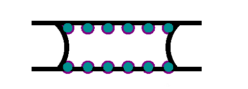
3. Requirements for stamp hole links
In the layout of a PCB, the number of link bars should be appropriate, generally 2-3 link bars, so that the strength of the PCB meets the requirements of the production process, do not break it at every turn.
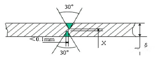
As shown in Figure 1-5, when designing the link bar, it is generally necessary to design a length of 4-5mm, the hole is non-metalized, the size is generally 0.3mm-0.5mm, and the distance between the holes is 0.8-1.2mm;
What to pay attention to in PCB design
Figure 1-5 Link bar design
4, craft side
When the board is more dense and the board edge space is limited, it is necessary to increase the process edge, which is used for the PCB board transfer edge when SMT, generally 3-5mm. Generally, a positioning hole is added to each of the four corners of the craft side, and optical positioning points are added to the three corners to strengthen the positioning of the machine, as shown in Figure