The Chinese name of PCB is printed circuit board, also known as printed circuit board. It is an important electronic component, a support for electronic components, and a carrier for electrical connection of electronic components. Because it is made using electronic printing, it is called a "printed" circuit board.
PCB classification
There are three main types of PCB boards:
1.Single PCB board
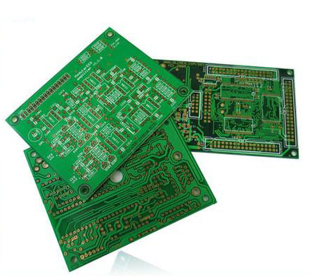
The single panel is on the most basic PCB. The parts are concentrated on one side, and the wires are concentrated on the other side (when there is a patch component, it is on the same side as the wire, and the plug-in device is on the other side).
2.Double PCB board
Double-sided board This type of circuit board has wiring on both sides, but to use the wires on both sides, you must have a proper circuit connection between the two sides.
3.Multilayer PCB board
In order to increase the wiring area, multi-layer boards use more single- or double-sided wiring boards.
Third, PCB characteristics
The reason why PCB can be used more and more widely, because it has many unique advantages, is as follows.
1. High density.
For decades, the high density of printed boards has been able to evolve with the integration of integrated circuits and advances in mounting technology.
Type of PCB
The classification of PCBs is generally divided by the number of layers, which are mainly divided into: single layer, double layer, and multi-layer.
1.Single-layer PCB
A single-layer PCB is also the most basic PCB. The parts are concentrated on one side and the wires are concentrated on the other side. Because single-layer PCBs have many strict restrictions on the design circuit (because there is only one side, the wiring cannot cross and must go around its own path), only early circuits used this type of PCB.
2.Double-layer PCB
The double-layer PCB has wiring on both sides. However, the two-sided wires are used to connect the circuit through the vias between the two layers. Because the area of the double-layer PCB is double that of the single-layer PCB, and because the wiring can be staggered (can be wound to the other side), it is more suitable for more complicated circuits than the single-layer PCB.
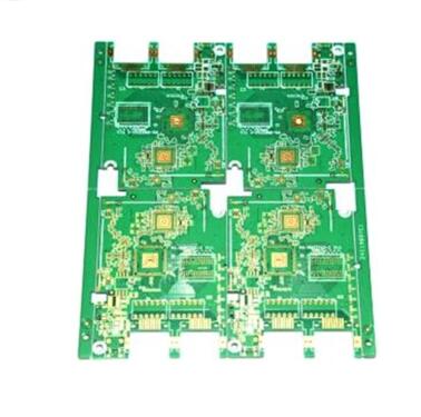
3.Multilayer PCB
In order to increase the area that can be routed, multi-layer PCBs use more single or double-layer wiring boards. Multi-layer PCB uses several double-sided boards, and puts an insulating layer between each board and presses it together. The number of layers of the PCB represents several independent wiring layers. Usually the number of layers is even and includes the two outermost layers. Most motherboards have a 4-8 layer structure. Because the layers in the PCB are tightly coupled, it is generally not easy to see the actual number.
In multilayer boards, more buried and blind via technologies are used. Because the vias mentioned in the double-layer PCB must penetrate the entire PCB. In a multi-layer PCB, if you only want to connect some of the lines, the vias may waste some other layers of wiring space. Buried and blind via technologies only penetrate a few of these layers. Blind vias connect several layers of the internal PCB to the surface PCB without having to penetrate the entire PCB. The buried hole is only connected to the internal PCB, so it cannot be seen from the surface.
